Control Panel: Scaffold
Public Unreviewedby Caleb
Control Panel: Scaffold — power and I/O dock board for the Adom workcell scaffold. Docks to the Control Panel: Workcell via a Samtec ET60T blade connector, delivering three isolated supply rails (+PS1 0–60 V/12 A, +PS2 5 V/10 A switched, +PS3), USB 2.0, debug, and 26 RP2350 USER_IO lines to a 65-contact machine field. Hosts the RP2350A Mini MCU molecule; role-aware USB-C (TUSB321 + TPS25940) sources PS2-derived VBUS as host and blocks back-feed as device; JP1–JP3 bond each isolated −PSx return t
Control Panel: Scaffold
Mated system — Workcell + Scaffold
The full Control Panel pair mated coplanar at the ET60 dock, with every nested molecule, jumper, and wire dropping in:
 Power and I/O dock board for the Adom workcell scaffold — the user-facing half of the Control Panel pair. It docks to the Control Panel: Workcell (CM5 carrier) through a Samtec ET60T blade connector and lands three isolated supply rails, USB 2.0, debug, and 26 RP2350 USER_IO lines on a 65-contact machine field where user electronics are built.
How It Works
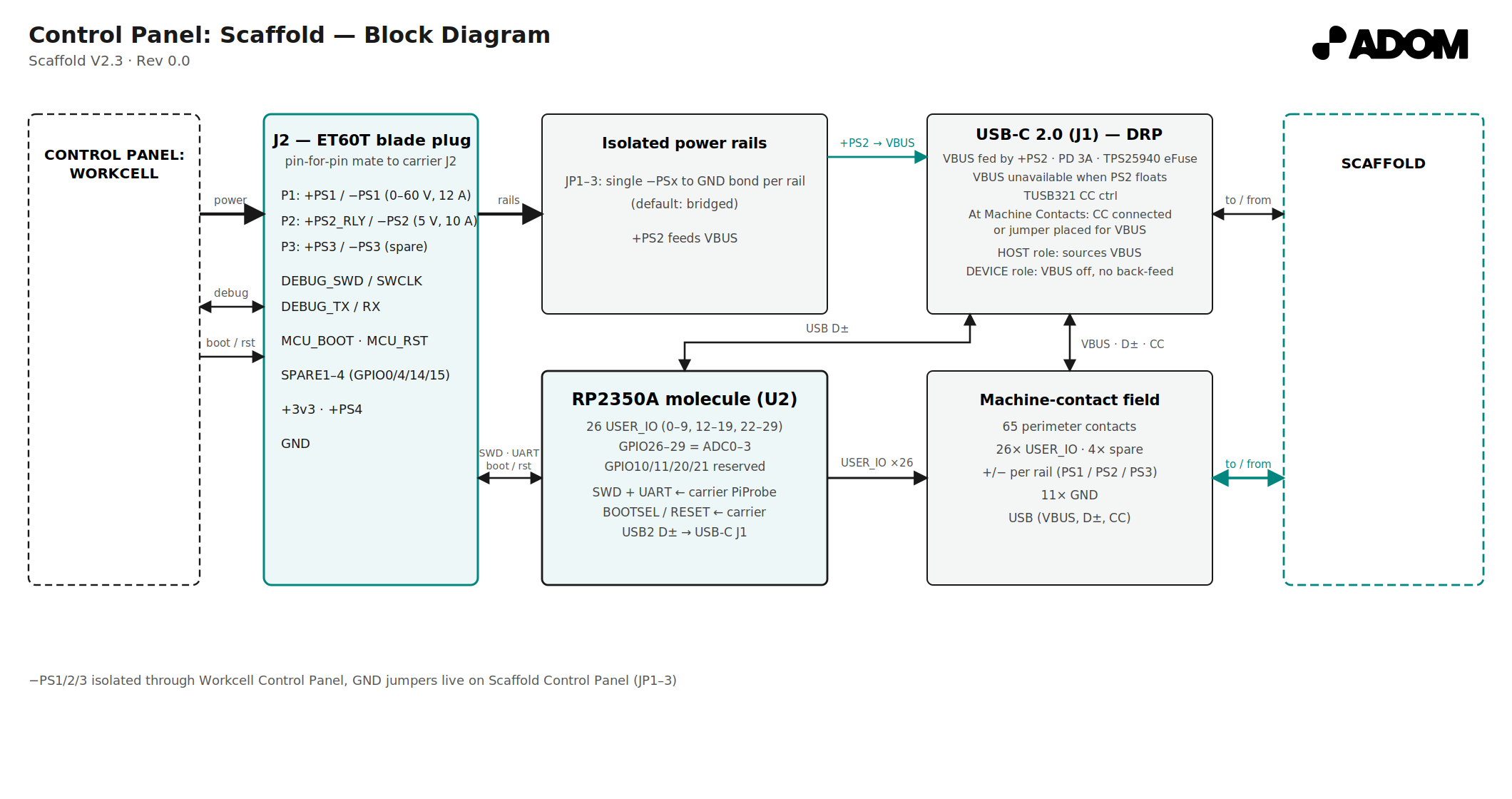
The Workcell feeds the Scaffold through the ET60T dock: power blades P1 (+PS1, 0–60 V / 12 A), P2 (+PS2, 5 V / 10 A, switched — "CM5 Enabled") and P3 (+PS3), plus SWD/UART debug, MCU boot/reset control, four spare CM5 GPIO, and +3v3/+PS4 service power. Each rail's return (−PS1/2/3) arrives isolated; JP1–JP3 large machine-pin jumper fields bond a single −PSx to GND per rail (default: bridged). The hosted RP2350A Mini molecule (U2) provides the user MCU — its 26 USER_IO route to the machine-contact field alongside the power rails, grounds, spares, and USB.
The USB-C port (J1) is dual-role with role-gated VBUS: as host, the TUSB321 (U3) ID output turns on Q1 (AO3401A) and the board sources VBUS from +PS2 through the TPS25940 eFuse (U1); as device (e.g. plugged into a PC for UF2/CDC), VBUS sourcing is off and the eFuse blocks back-feed into PS2. PD advertisement is 3.0 A. For VBUS delivery at the machine contacts, connect the CC contact or place the CC jumper (JP4). U4 (TPD2EUSB30) provides USB ESD protection.
Overview
| Property | Value |
|---|---|
| Molecule ID | control-panel-scaffold |
| Board Size | 160.0 × 45.0 mm |
| Dock | Samtec ET60T-S03 — 3 power blades + 60 signal pins, to Control Panel: Workcell |
| User MCU | RP2350A Mini molecule (U2 slot) — 26 USER_IO (GPIO10/11/20/21 reserved) |
| Machine field | 65 contacts (62 medium + 3 large) |
| USB | USB-C 2.0 dual-role, PD 3.0 A, role-gated VBUS from +PS2 |
| Ground scheme | JP1–JP3: single −PSx↔GND bond per rail (large machine-pin jumpers, default bridged) |
| Mounting | 6× M3 (3.2 mm NPTH) |
| KiCad Version | 8 |
Companion Documents
Bundled on this page's release as Control_Panel_Scaffold_Companion_Docs.zip; individual copies are downloadable assets on the board pages' releases:
| Document | Purpose |
|---|---|
| Scaffold Functionality Overview | Function tables, RP2350 pin tree, block diagram |
| Control Panel Functionality Overview | The Workcell-side companion overview |
| Control Panel Test Procedure | Bring-up/test steps — Scaffold is §9 |
| Control Panel Test Method Overview | Record sheet used with the procedure |
| Scaffold block diagram | This page's diagram, print form |
| Workcell block diagram | System-side diagram |
| Rev notes | Board revision history |
Key ICs
| Ref | Part | Function |
|---|---|---|
| U1 | TPS25940 | USB VBUS eFuse (+PS2 → VBUS, back-feed blocking) |
| U2 | RP2350A Mini molecule | User MCU (hosted molecule slot) |
| U3 | TUSB321 | USB-C CC controller — role detect, ID-gated VBUS |
| U4 | TPD2EUSB30 | USB D± ESD protection |
| Q1 | AO3401A | P-FET VBUS source switch (host role) |
Jumpers
| Ref | Field | Function |
|---|---|---|
| JP1 | 12×6 large machine pins | −PS1 ↔ GND bond (default bridged) |
| JP2 | 12×6 large machine pins | −PS2 ↔ GND bond (default bridged) |
| JP3 | 12×6 large machine pins | −PS3 ↔ GND bond (default bridged) |
| JP4 | 2-pad | CC jumper — enables VBUS at the machine contacts without a CC-wired device |
Machine Contact Pin Mapping
Power rails
| Contacts | Net | Notes |
|---|---|---|
| MC1–MC4 | +PS1_SENS | PS1 rail (0–60 V, 12 A), sense-tapped |
| MC5–MC8 | +PS2_RLY | PS2 rail (5 V, 10 A, switched) |
| MC9–MC12 | +PS3 | PS3 rail (blade P3) |
| MC22–MC24 | −PS1 | isolated return, bonded via JP1 |
| MC25–MC27 | −PS2 | isolated return, bonded via JP2 |
| MC28–MC30 | −PS3 | isolated return, bonded via JP3 |
| MC13–MC14, MC57–MC65 | GND |
USB & spares
| Contacts | Net | Notes |
|---|---|---|
| MC15 | USB2_VBUS | VBUS at the field (see JP4 / CC) |
| MC16 | MCU_USB2_D+ | RP2350 USB |
| MC17 | MCU_USB2_D− | RP2350 USB |
| MC18–MC21 | SPARE1–SPARE4 | CM5 spare GPIO (0 / 4 / 14 / 15) from the dock |
USER_IO (RP2350A Mini)
| Contacts | Net |
|---|---|
| MC31–MC38 | USER_IO 29, 28, 27, 26, 25, 24, 23, 22 |
| MC39–MC46 | USER_IO 19, 18, 17, 16, 15, 14, 13, 12 |
| MC47–MC56 | USER_IO 9, 8, 7, 6, 5, 4, 3, 2, 1, 0 |
26 USER_IO total — RP2350 GPIO10/11/20/21 are reserved on the Mini and never reach the field.
3D Model / Bundle
Control_Panel_Scaffold_v2.0.1.glb— OCCT conversion of the design-machine STEP (the Mini molecule is modeled docked in its slot)control-panel_scaffold_v2.0.1.step/.kicad_pcb/.kicad_sch/.kicad_pro— sources- JLCPCB BOM / CPL / gerbers
This board is a dock base — it carries no MP anchor markers of its own (molecules dock onto it), so the GLB is a standard component conversion; wire-attach data for Hydrogen is generated from the board at import.
Import
adom-molecule create with --no-optimize reusing this GLB — do not regenerate from EDA export.
# Control Panel: Scaffold
## Mated system — Workcell + Scaffold
The full Control Panel pair mated coplanar at the ET60 dock, with every nested molecule, jumper, and wire dropping in:

Power and I/O dock board for the Adom workcell scaffold — the user-facing half of the Control Panel pair. It docks to the **Control Panel: Workcell** (CM5 carrier) through a Samtec ET60T blade connector and lands three isolated supply rails, USB 2.0, debug, and 26 RP2350 USER_IO lines on a 65-contact machine field where user electronics are built.

## How It Works
The Workcell feeds the Scaffold through the ET60T dock: power blades P1 (+PS1, 0–60 V / 12 A), P2 (+PS2, 5 V / 10 A, switched — "CM5 Enabled") and P3 (+PS3), plus SWD/UART debug, MCU boot/reset control, four spare CM5 GPIO, and +3v3/+PS4 service power. Each rail's return (−PS1/2/3) arrives isolated; **JP1–JP3 large machine-pin jumper fields bond a single −PSx to GND per rail** (default: bridged). The hosted **RP2350A Mini molecule** (U2) provides the user MCU — its 26 USER_IO route to the machine-contact field alongside the power rails, grounds, spares, and USB.
The USB-C port (J1) is dual-role with role-gated VBUS: as **host**, the TUSB321 (U3) ID output turns on Q1 (AO3401A) and the board sources VBUS from +PS2 through the TPS25940 eFuse (U1); as **device** (e.g. plugged into a PC for UF2/CDC), VBUS sourcing is off and the eFuse blocks back-feed into PS2. PD advertisement is 3.0 A. For VBUS delivery at the machine contacts, connect the CC contact or place the CC jumper (JP4). U4 (TPD2EUSB30) provides USB ESD protection.
## Overview
| Property | Value |
|---|---|
| **Molecule ID** | `control-panel-scaffold` |
| **Board Size** | 160.0 × 45.0 mm |
| **Dock** | Samtec ET60T-S03 — 3 power blades + 60 signal pins, to Control Panel: Workcell |
| **User MCU** | RP2350A Mini molecule (U2 slot) — 26 USER_IO (GPIO10/11/20/21 reserved) |
| **Machine field** | 65 contacts (62 medium + 3 large) |
| **USB** | USB-C 2.0 dual-role, PD 3.0 A, role-gated VBUS from +PS2 |
| **Ground scheme** | JP1–JP3: single −PSx↔GND bond per rail (large machine-pin jumpers, default bridged) |
| **Mounting** | 6× M3 (3.2 mm NPTH) |
| **KiCad Version** | 8 |
## Companion Documents
Bundled on this page's release as
[Control_Panel_Scaffold_Companion_Docs.zip](/download/caleb/control-panel-scaffold/2.0.2/Control_Panel_Scaffold_Companion_Docs.zip);
individual copies are downloadable assets on the board pages' releases:
| Document | Purpose |
|---|---|
| [Scaffold Functionality Overview](/download/caleb/control-panel-scaffold/2.0.22/Scaffold_Functionality_Overview_v0.0.pdf) | Function tables, RP2350 pin tree, block diagram |
| [Control Panel Functionality Overview](/download/caleb/control-panel-workcell/2.0.19/Control_Panel_Functionality_Overview_v0.0.pdf) | The Workcell-side companion overview |
| [Control Panel Test Procedure](/download/caleb/control-panel-workcell/2.0.19/Control_Panel_Test_Procedure.pdf) | Bring-up/test steps — Scaffold is §9 |
| [Control Panel Test Method Overview](/download/caleb/control-panel-workcell/2.0.19/Control_Panel_Test_Method_Overview.pdf) | Record sheet used with the procedure |
| [Scaffold block diagram](/download/caleb/control-panel-scaffold/2.0.22/scaffold-block-diagram_v0.0.pdf) | This page's diagram, print form |
| [Workcell block diagram](/download/caleb/control-panel-workcell/2.0.19/control-panel-block-diagram_v0.0.pdf) | System-side diagram |
| [Rev notes](docs/Control_Panel_Scaffold_Rev_Notes.txt) | Board revision history |
## Key ICs
| Ref | Part | Function |
|---|---|---|
| U1 | TPS25940 | USB VBUS eFuse (+PS2 → VBUS, back-feed blocking) |
| U2 | RP2350A Mini molecule | User MCU (hosted molecule slot) |
| U3 | TUSB321 | USB-C CC controller — role detect, ID-gated VBUS |
| U4 | TPD2EUSB30 | USB D± ESD protection |
| Q1 | AO3401A | P-FET VBUS source switch (host role) |
## Jumpers
| Ref | Field | Function |
|---|---|---|
| JP1 | 12×6 large machine pins | −PS1 ↔ GND bond (default bridged) |
| JP2 | 12×6 large machine pins | −PS2 ↔ GND bond (default bridged) |
| JP3 | 12×6 large machine pins | −PS3 ↔ GND bond (default bridged) |
| JP4 | 2-pad | CC jumper — enables VBUS at the machine contacts without a CC-wired device |
## Machine Contact Pin Mapping
### Power rails
| Contacts | Net | Notes |
|---|---|---|
| MC1–MC4 | +PS1_SENS | PS1 rail (0–60 V, 12 A), sense-tapped |
| MC5–MC8 | +PS2_RLY | PS2 rail (5 V, 10 A, switched) |
| MC9–MC12 | +PS3 | PS3 rail (blade P3) |
| MC22–MC24 | −PS1 | isolated return, bonded via JP1 |
| MC25–MC27 | −PS2 | isolated return, bonded via JP2 |
| MC28–MC30 | −PS3 | isolated return, bonded via JP3 |
| MC13–MC14, MC57–MC65 | GND | |
### USB & spares
| Contacts | Net | Notes |
|---|---|---|
| MC15 | USB2_VBUS | VBUS at the field (see JP4 / CC) |
| MC16 | MCU_USB2_D+ | RP2350 USB |
| MC17 | MCU_USB2_D− | RP2350 USB |
| MC18–MC21 | SPARE1–SPARE4 | CM5 spare GPIO (0 / 4 / 14 / 15) from the dock |
### USER_IO (RP2350A Mini)
| Contacts | Net |
|---|---|
| MC31–MC38 | USER_IO 29, 28, 27, 26, 25, 24, 23, 22 |
| MC39–MC46 | USER_IO 19, 18, 17, 16, 15, 14, 13, 12 |
| MC47–MC56 | USER_IO 9, 8, 7, 6, 5, 4, 3, 2, 1, 0 |
26 USER_IO total — RP2350 GPIO10/11/20/21 are reserved on the Mini and never reach the field.
## 3D Model / Bundle
- `Control_Panel_Scaffold_v2.0.1.glb` — OCCT conversion of the design-machine STEP (the Mini molecule is modeled docked in its slot)
- `control-panel_scaffold_v2.0.1.step` / `.kicad_pcb` / `.kicad_sch` / `.kicad_pro` — sources
- JLCPCB BOM / CPL / gerbers
This board is a dock **base** — it carries no MP anchor markers of its own (molecules dock onto it), so the GLB is a standard component conversion; wire-attach data for Hydrogen is generated from the board at import.
## Import
`adom-molecule` create with `--no-optimize` reusing this GLB — do not regenerate from EDA export.