RITHESH LED Display
Public Unreviewedby Rithesh03
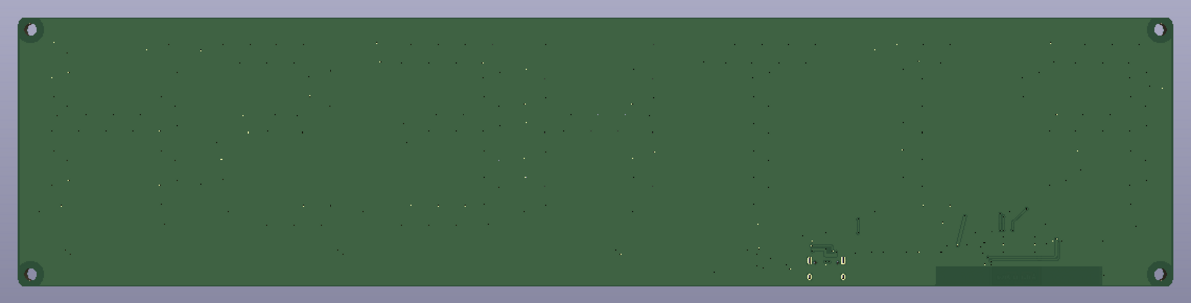
A 300 x 70 mm PCB that spells RITHESH with 107 WS2812B RGB LEDs, controlled over Wi-Fi.

Datasheet
Open in new tab ↗Contents
README
markdownRITHESH LED Display
A custom circuit board that spells the name RITHESH with 107 colour LEDs. You control it from a phone or computer over Wi-Fi, using the free WLED app. It is powered from an ordinary USB-C phone charger.
Status (2026-09-25): Version 1 design complete and approved for a prototype. Not ordered yet. Two things must pass first: a timing test with a few real LEDs, and JLCPCB's manufacturing review. A smaller Version 2 is being planned (see the last section).

Project overview
- What it is: a 300 × 70 mm board with the letters R-I-T-H-E-S-H made of small addressable RGB LEDs. Every LED can show any colour.
- Why: a personal name sign that can show colours, patterns and animations, controlled from a phone.
- How it was made: requirements, schematic, PCB layout and every check were done step by step and saved in this page's files. The board is designed for JLCPCB to make and assemble (all parts soldered by the factory).
Final Version 1 specifications
| Size | 300 × 70 mm, 2 layers, 1.6 mm thick, 1 oz copper, four M3 mounting holes |
| LEDs | 107 × XL-5050RGBC-2812B (WS2812B-style), 5 × 5 mm, 7 mm apart, each with its own 100 nF capacitor |
| Letters | 5 × 7 dot pattern, each letter about 33 × 47 mm |
| Brain | ESP32-C3-MINI-1 Wi-Fi module running standard WLED |
| Power | USB-C, 5 V, up to 3 A charger. WLED limits the whole board to 2 A |
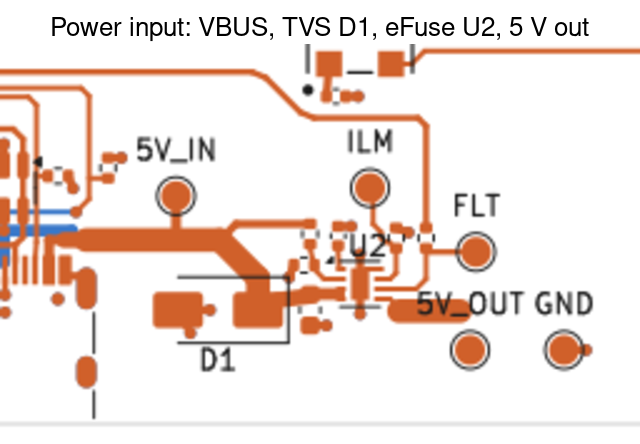
| Protection | surge diode, USB protection chip, and an electronic fuse (eFuse) with soft start, current limit and over-voltage clamp |
| Buttons | RESET, ON/OFF, BOOT |
| Test pads | 10 (power, 3.3 V, ground, LED data, eFuse status and current, serial RX/TX) |
| Assembly | 250 parts, all on the front |
How the board works
- The USB-C charger supplies 5 V.
- A surge diode and a USB protection chip absorb voltage spikes, and the eFuse switches the power on gently and cuts it off if too much current flows (about 2.5–2.9 A) or the voltage is too high.
- A 3.3 V regulator powers the ESP32-C3 Wi-Fi chip.
- The ESP32 runs WLED. It sends colour data out of one pin (GPIO10).
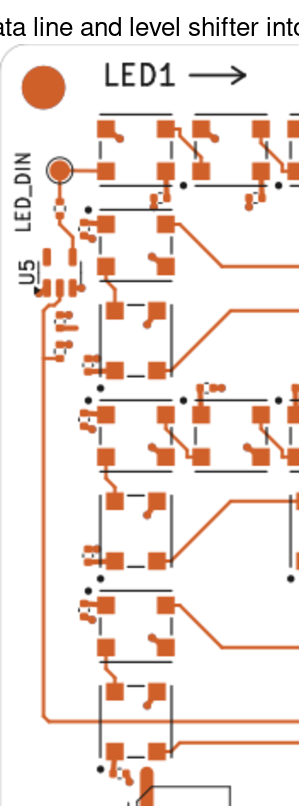
- A level shifter turns the 3.3 V data signal into a clean 5 V signal for the LEDs.
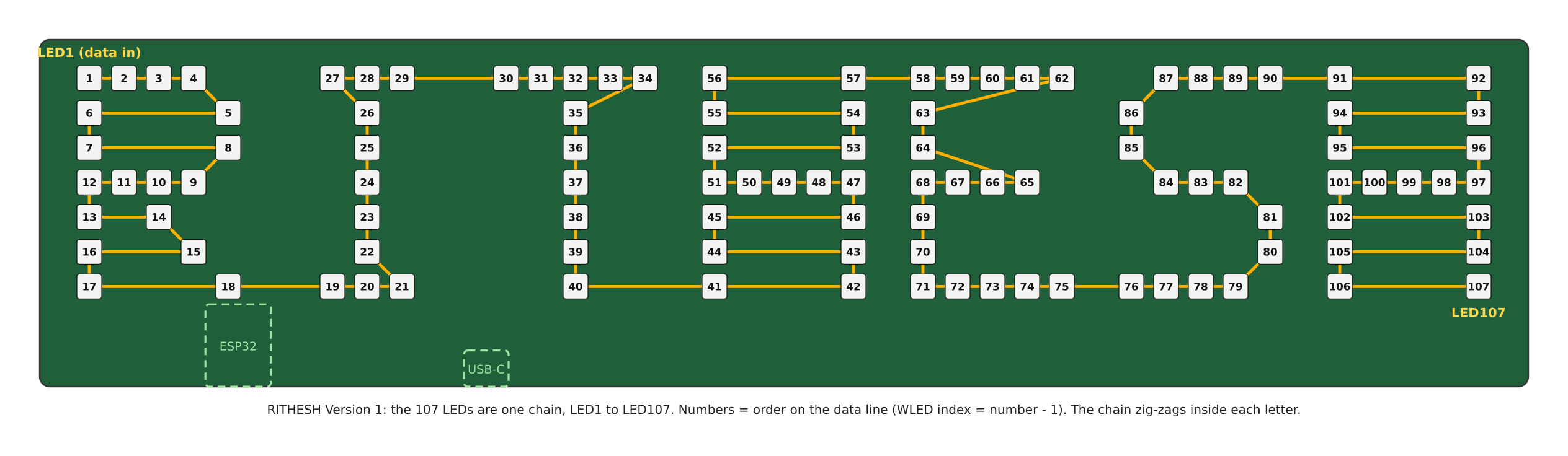
- The data enters LED1 (top-left of the "R") and passes from LED to LED, all the way to LED107.
Major components
| Part | What it does | JLCPCB part |
|---|---|---|
| XL-5050RGBC-2812B × 107 | the colour LEDs (WS2812B-style, each with a tiny built-in controller) | C2843785 |
| ESP32-C3-MINI-1-N4 | Wi-Fi chip that runs WLED; also programmed over the USB-C port | C2838502 |
| TPS259531 eFuse | soft start, 2.5–2.9 A current limit, over-voltage clamp, automatic restart after a fault | C2155674 |
| SMAJ5.0A | surge (TVS) diode on the 5 V input | C2925443 |
| USBLC6-2SC6 | protects the USB data lines from static | C7519 |
| TLV76733 | 3.3 V regulator for the ESP32 | C2848334 |
| SN74AHCT1G125 | 3.3 V to 5 V level shifter for the LED data | C7484 |
| TYPE-C-31-M-12 | USB-C connector for power and programming | C165948 |
| 220 µF × 2 (+ 2 spare spots) | bulk capacitors that steady the LED power | C72496 |
Power design
- Budget: the charger gives up to 3 A. WLED keeps the whole board at or under 2 A (about 1.88 A for the LEDs plus the ESP32).
- Full white: all LEDs at full white would need about 3.85 A, so WLED dims white to about 30 %. Single colours can be much brighter.
- Supply copper: the back of the board is a solid ground plane. The front has a 5 V copper area under all the LEDs.
- Voltage drop: the worst voltage loss to the farthest LED is calculated at only 9 mV at 1.88 A.
- eFuse: stays below the charger's 3 A and above the board's 2.2 A worst case (including Wi-Fi peaks).

PCB design and checks
- Checks that all pass:
- design-rule check: 0 errors, 0 unconnected, 0 footprint errors
- electrical-rule check: 0 errors, 0 warnings
- every chip pin checked against its datasheet
- netlist checker, placement checker and a voltage-drop calculation
- Antenna: the ESP32 antenna sits at the bottom edge with no copper under or beside it.
- USB: the data pair has protection right at the connector and ground vias wherever it changes layer.
- Vias: all are covered by solder mask, and none are inside a pad.
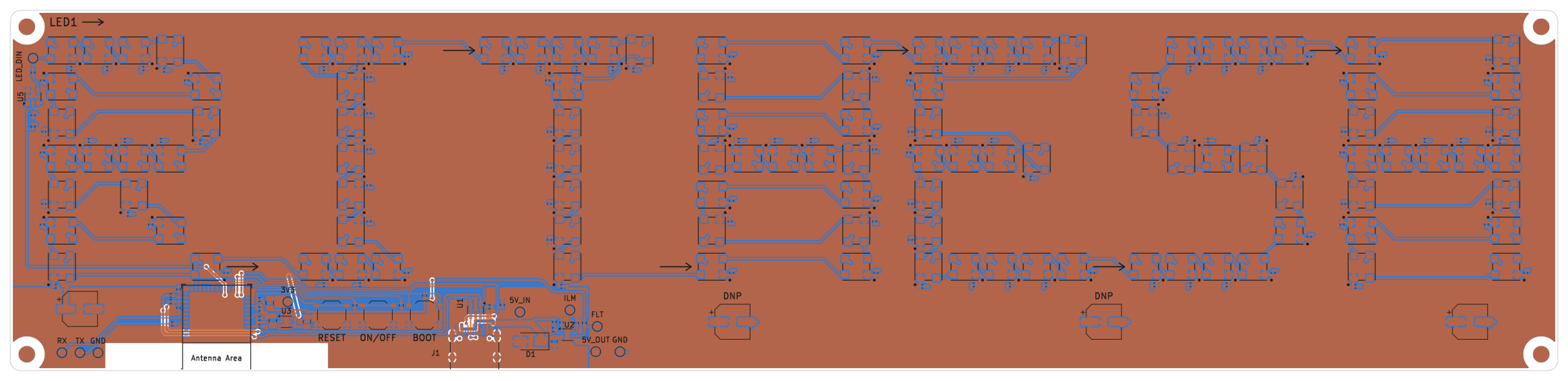

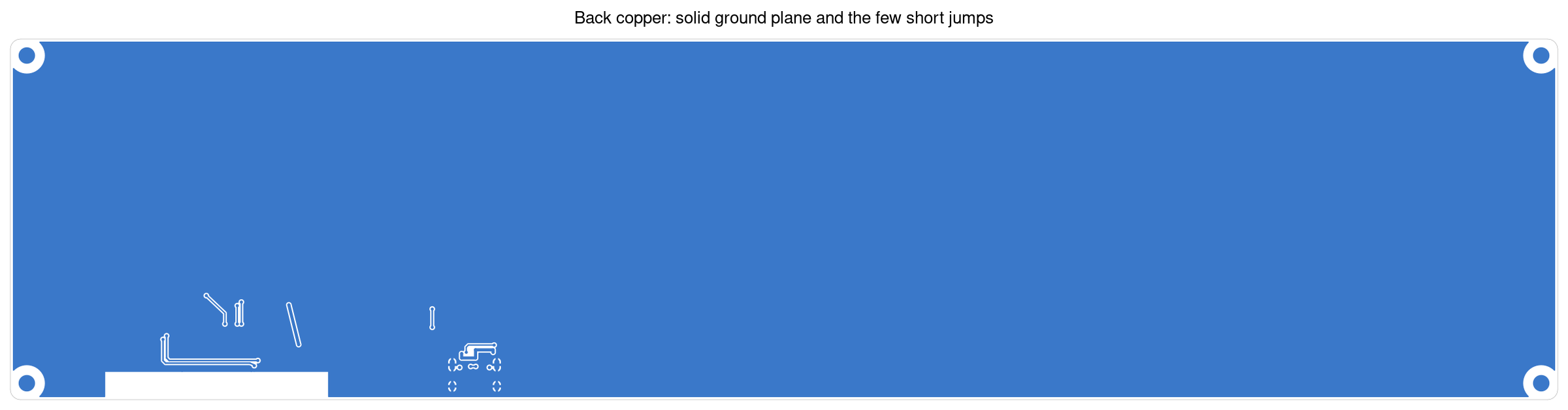

Design notes: hardware/pcb-layout-notes.md · schematic: hardware/schematic.pdf · all decisions: requirements.md
Firmware and WLED
- Firmware: standard WLED, installed from a web browser at install.wled.me. No custom firmware is needed.
- Settings:
- LED output on GPIO10, 107 LEDs
- ON/OFF button on GPIO5
- Maximum PSU Current 2000 mA
- Letter effects: the files
firmware/ledmap.jsonandfirmware/ledmap1.jsonmake effects follow the letters. - Full guide: firmware/README.md covers installing, Wi-Fi setup, testing and USB recovery.
Manufacturing package
hardware/manufacturing/RITHESH-v1-PROTOTYPE/ contains:
- the Gerber and drill ZIP
- the parts list (BOM) and placement file (CPL) for JLCPCB
- assembly drawings and fabrication notes
It is marked "PROTOTYPE – DO NOT ORDER" until the tests below pass. Nothing has been uploaded to JLCPCB or ordered.
Remaining physical tests
Before ordering:
- LED timing test: 5–10 real LEDs on an ESP32-C3 running WLED for 30 minutes, plus an oscilloscope check of the data timing.
- JLCPCB review:
- manufacturing check
- placement preview (every part's rotation and pin 1)
- stock
- board size accepted
- final price
On the prototype:
- Power: starts cleanly; 5 V stays at or above 4.7 V at full load.
- LEDs: all 107 light in the right order.
- WLED: the 2 A limit holds.
- Connections: Wi-Fi range, USB programming and the RESET/BOOT recovery, and the ON/OFF button all work.
- Power ripple: decides whether to fit the two spare capacitors.
The full list is in FINAL-REVIEW-CHECKLIST.md.
Version 2 optimization plan
A smaller Version 2 is being planned in v2/. It is a proposal only; Version 1 stays unchanged.
| Version 1 | Version 2 (plan) | |
|---|---|---|
| Board | 300 × 70 mm | 250 × 40 mm (about half the area) |
| LEDs | 107 × 5 mm LEDs, 7 mm apart | 107 × 2 mm LEDs, 5 mm apart |
| Letters | 33 × 47 mm | 22 × 32 mm |
| Full white | about 3.85 A (dimmed by WLED) | about 1.66 A (full brightness) |
| Electronics | strip under the letters | at the right end |
In Version 2 the LED data enters at the right end, next to the electronics. The letters look the same, but the LED numbering is reversed: V2 LED1 is where V1 LED107 is. Version 2 therefore has its own WLED maps in v2/firmware/.
The new LED stays provisional until its own timing test passes. Details are in v2/requirements.md.
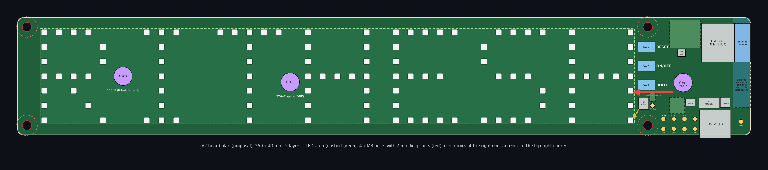
Files: README · requirements · updates · final checklist · Hydrogen feedback