JST Connector Studio: manufacturer 3D mate editor
Public Unreviewedby John Lauer
Interactive Babylon 9.5 studio for JST wire-to-board connectors: load a system (PH/XH/SH/GH/ZH), see the JST manufacturer housing+wire+ds2sf footprint mate in a looping animation next to the KiCad hou
name: jst-connector-cad description: Source JST connector manufacturer CAD (email-gated STEP) and build interactive, animated, footprint-accurate wiki component pages — board+wire mate animation, true-scale pads registered to real pins, KiCad-vs-JST comparison, and the Babylon-viewer gotchas. Use when working with JST connectors, manufacturer 3D/STEP, ds2sf footprints, or animated GLB component pages.
JST connector CAD — manufacturer 3D + animated mating component pages
A reproducible recipe for sourcing JST connector CAD the manufacturer-first way and turning it into an interactive, animated, footprint-accurate wiki component page. Built and verified end-to-end (PH/XH/SH/GH/ZH 2-circuit systems).
The point of chip-fetcher: the 3D model is the manufacturer's (JST's own STEP). KiCad is used only for the redistributable symbol/footprint and as a side-by-side comparison foil — never as the 3D deliverable.
1. Get the manufacturer CAD (email-gated)
JST gates STEP downloads behind an email form on jst-mfg.com, and jst.com (USA)
Cloudflare-walls headless browsers. Drive the user's real browser (native-browser
bridge), fill the License Agreement form, and retrieve the emailed STEP via the Gmail API
(adom-google). One submit per file; dedupe; trash demo emails. Full flow:
chip-fetcher playbooks jst.md + jst-email-retrieval.md.
For each 2-circuit system you want three real parts: board header, wire housing, crimp contacts — plus the KiCad symbol/footprint (and KiCad 3D if it exists).
2. Mating orientation (which way the wire goes in)
Encoded in the part number AND the datasheet drawing:
B…(B2B, BM) = top entry → wire mates straight down (+Z).S…(SM, S2B) = side entry / right-angle → wire mates horizontally (+Y).
3. STEP → GLB
step2glb convert each STEP. It emits Draco-compressed GLB that trimesh can't read —
decompress with @gltf-transform (unpartition + dispose KHR_draco_mesh_compression).
Use step2glb features / thumbnail --pose front|top|side to read each model's pin axis;
KiCad models are reliably Z-up, pins −Z (identity), JST THT boards here needed R_x(+90).
4. Compose the scene (trimesh) — the part that matters
Two columns: KiCad foil (tan/grey) | JST manufacturer (blue). One column if KiCad has no 3D.
Seat the body, not the bbox. The connector's body bottom (where the cross-section
widens above the thin pins) sits on the PCB top. Seating by bbox.min sinks the housing
into the PCB. Detect body-bottom by walking z-slices for the first wide slice.
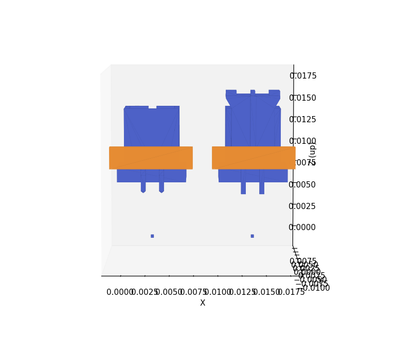
True-scale footprint pads, registered to the real pins. Do not paste the footprint
as a scaled image — its pads won't land on the pins. Parse the .kicad_mod, render copper
pads (THT = ring + drill hole, SMT = roundrect) at real mm coords, then register:
detect the connector's pin centroid + axis from the mesh's lowest band and rotate/translate
the pads onto them. Validate numerically: pad_pitch == pin_pitch (e.g. PH 2.0 == 2.0).
This is what makes pins land in holes:
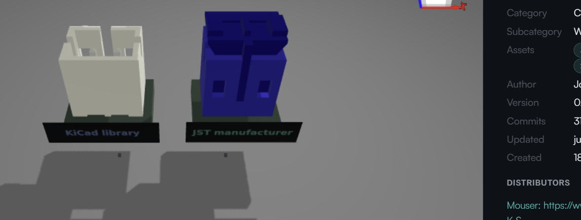
Float the PCB; show pins through. Render the PCB as a thin (~1.6 mm) slab at ~8 mm, no riser (a riser hides the underside). THT boards seat with pins through the slab and protruding out the bottom. Drop a tiny (~0.3 mm) invisible anchor at z=0 so the viewer (which grounds to the lowest geometry) puts the floor low and you can look under the PCB:
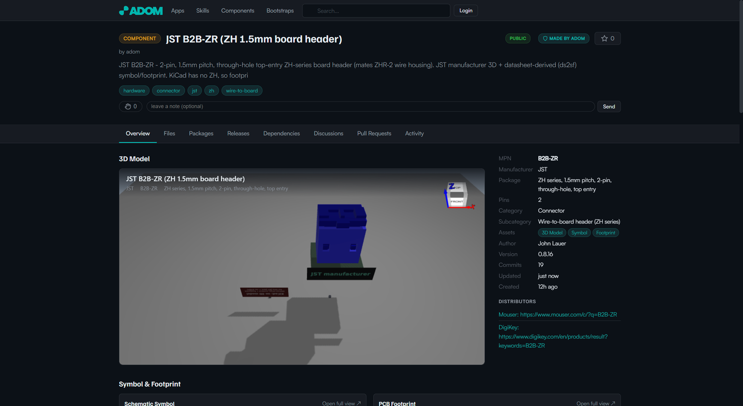
If KiCad has no 3D model (e.g. ZH B2B-ZR → kicad-packages3d 404), don't silently
drop the column — stand a red "KiCad: no 3D model" placard in its slot:
5. Animate (GLB node channels)
Name the board/wire nodes; bake geometry at the seated pose (node base TRS = seated, so
a non-animating viewer still looks right). Add an animation with @gltf-transform
(createAnimationSampler/createAnimationChannel, path translation, LINEAR): board
descends so pins pass through, then the wire inserts ~80% into the board body
(shows JST's contact slots). Keep lifts small; dwell long on the fully-mated state (the
money shot), quick reset, loop. The Babylon viewer autoplays + loops embedded GLB
animations — no play button.
6. Babylon-viewer gotchas (these cost real time — verify, don't assume)
- ALWAYS screenshot your own generated 3D view in the live viewer and READ it. matplotlib renders geometry but not textures/text, so it will not reveal mirrored/upside-down labels or texture issues. Only the real Babylon viewer tells the truth.
- The 3D viewer is an
<iframe>(/viewer/3d/component/<slug>). Reloading the parent page does not refresh the iframe's cached GLB. Bump the GLB filename (-vN.glb) and/or setiframe.src += '?cb=…'. - Texture orientation: on these quads Babylon maps UV so image-top lands at the quad
bottom (use uv
[[0,1],[1,1],[1,0],[0,0]]for upright) and flips U on the camera-facing face (pre-mirror the image withImageOps.mirror). For two-sided labels use separated single-winding quads (coplanar double-winding z-fights), both pre-mirrored, backed opaque (transparent PNGs bleed through). - bbox-check everything and print it: body-bottom on PCB top, pins protrude, pad_pitch == pin_pitch, wire above PCB. Cheap asserts catch the geometry bugs.
- Publish: components/skills are org-owned —
adompkg publish --org adom(publishing as your user 409s).
Live examples (the 5 built with this recipe)
B2B-PH-K-S (PH 2.0) · B2B-XH-A (XH 2.5) · SM02B-SRSS-TB (SH 1.0, side-entry) · BM02B-GHS-TBT (GH 1.25 SMT) · B2B-ZR (ZH 1.5, no KiCad 3D)
See also: chip-fetcher.
---
name: jst-connector-cad
description: Source JST connector manufacturer CAD (email-gated STEP) and build interactive, animated, footprint-accurate wiki component pages — board+wire mate animation, true-scale pads registered to real pins, KiCad-vs-JST comparison, and the Babylon-viewer gotchas. Use when working with JST connectors, manufacturer 3D/STEP, ds2sf footprints, or animated GLB component pages.
---
# JST connector CAD — manufacturer 3D + animated mating component pages
A reproducible recipe for sourcing **JST** connector CAD the manufacturer-first way and
turning it into an **interactive, animated, footprint-accurate** wiki component page. Built
and verified end-to-end (PH/XH/SH/GH/ZH 2-circuit systems).
> **The point of chip-fetcher:** the **3D model is the manufacturer's** (JST's own STEP).
> KiCad is used **only** for the redistributable symbol/footprint and as a side-by-side
> *comparison foil* — never as the 3D deliverable.
## 1. Get the manufacturer CAD (email-gated)
JST gates STEP downloads behind an email form on `jst-mfg.com`, and `jst.com` (USA)
Cloudflare-walls headless browsers. Drive the user's **real** browser (native-browser
bridge), fill the License Agreement form, and retrieve the emailed STEP via the Gmail API
(`adom-google`). One submit per file; dedupe; trash demo emails. Full flow:
**chip-fetcher** playbooks `jst.md` + `jst-email-retrieval.md`.
For each 2-circuit system you want three real parts: **board header**, **wire housing**,
**crimp contacts** — plus the **KiCad symbol/footprint** (and KiCad 3D *if it exists*).
## 2. Mating orientation (which way the wire goes in)
Encoded in the part number AND the datasheet drawing:
- `B…` (B2B, BM) = **top entry** → wire mates **straight down (+Z)**.
- `S…` (SM, S2B) = **side entry / right-angle** → wire mates **horizontally (+Y)**.
## 3. STEP → GLB
`step2glb convert` each STEP. It emits **Draco-compressed** GLB that trimesh can't read —
decompress with `@gltf-transform` (`unpartition` + dispose `KHR_draco_mesh_compression`).
Use `step2glb features` / `thumbnail --pose front|top|side` to read each model's pin axis;
KiCad models are reliably **Z-up, pins −Z** (identity), JST THT boards here needed `R_x(+90)`.
## 4. Compose the scene (trimesh) — the part that matters
Two columns: **KiCad foil** (tan/grey) | **JST manufacturer** (blue). One column if KiCad
has no 3D.
**Seat the body, not the bbox.** The connector's *body bottom* (where the cross-section
widens above the thin pins) sits on the PCB top. Seating by `bbox.min` sinks the housing
**into** the PCB. Detect body-bottom by walking z-slices for the first wide slice.
**True-scale footprint pads, registered to the real pins.** Do **not** paste the footprint
as a scaled image — its pads won't land on the pins. Parse the `.kicad_mod`, render copper
pads (THT = ring + drill hole, SMT = roundrect) at real mm coords, then **register**:
detect the connector's pin centroid + axis from the mesh's lowest band and rotate/translate
the pads onto them. Validate numerically: `pad_pitch == pin_pitch` (e.g. PH 2.0 == 2.0).
This is what makes pins land in holes:

**Float the PCB; show pins through.** Render the PCB as a thin (~1.6 mm) slab at ~8 mm,
**no riser** (a riser hides the underside). THT boards seat with pins **through** the slab
and protruding out the bottom. Drop a tiny (~0.3 mm) **invisible anchor at z=0** so the
viewer (which grounds to the lowest geometry) puts the floor low and you can look **under**
the PCB:

**If KiCad has no 3D model** (e.g. ZH `B2B-ZR` → `kicad-packages3d` 404), don't silently
drop the column — stand a red **"KiCad: no 3D model"** placard in its slot:

## 5. Animate (GLB node channels)
Name the board/wire nodes; bake geometry at the **seated** pose (node base TRS = seated, so
a non-animating viewer still looks right). Add an animation with `@gltf-transform`
(`createAnimationSampler`/`createAnimationChannel`, path `translation`, LINEAR): board
descends so **pins pass through**, then the wire **inserts ~80%** into the board body
(shows JST's contact slots). Keep lifts small; **dwell long on the fully-mated state** (the
money shot), quick reset, loop. The Babylon viewer **autoplays + loops** embedded GLB
animations — no play button.
## 6. Babylon-viewer gotchas (these cost real time — verify, don't assume)
- **ALWAYS screenshot your own generated 3D view in the live viewer and READ it.** matplotlib
renders geometry but **not textures/text**, so it will not reveal mirrored/upside-down
labels or texture issues. Only the real Babylon viewer tells the truth.
- **The 3D viewer is an `<iframe>`** (`/viewer/3d/component/<slug>`). Reloading the parent
page does **not** refresh the iframe's cached GLB. Bump the GLB **filename** (`-vN.glb`)
and/or set `iframe.src += '?cb=…'`.
- **Texture orientation:** on these quads Babylon maps UV so image-top lands at the quad
**bottom** (use uv `[[0,1],[1,1],[1,0],[0,0]]` for upright) **and** flips U on the
camera-facing face (pre-mirror the image with `ImageOps.mirror`). For two-sided labels use
**separated** single-winding quads (coplanar double-winding z-fights), both pre-mirrored,
backed **opaque** (transparent PNGs bleed through).
- **bbox-check everything** and print it: body-bottom on PCB top, pins protrude, pad_pitch
== pin_pitch, wire above PCB. Cheap asserts catch the geometry bugs.
- **Publish:** components/skills are **org-owned** — `adompkg publish --org adom` (publishing
as your user 409s).
## Live examples (the 5 built with this recipe)
[B2B-PH-K-S (PH 2.0)](https://wiki.adom.inc/adom/b2b-ph-k-s) ·
[B2B-XH-A (XH 2.5)](https://wiki.adom.inc/adom/b2b-xh-a) ·
[SM02B-SRSS-TB (SH 1.0, side-entry)](https://wiki.adom.inc/adom/sm02b-srss-tb) ·
[BM02B-GHS-TBT (GH 1.25 SMT)](https://wiki.adom.inc/adom/bm02b-ghs-tbt) ·
[B2B-ZR (ZH 1.5, no KiCad 3D)](https://wiki.adom.inc/adom/b2b-zr)
See also: [chip-fetcher](https://wiki.adom.inc/adom/adom-chip-fetcher).