JST Connector Studio: manufacturer 3D mate editor
Public Unreviewedby John Lauer
Interactive Babylon 9.5 studio for JST wire-to-board connectors: load a system (PH/XH/SH/GH/ZH), see the JST manufacturer housing+wire+ds2sf footprint mate in a looping animation next to the KiCad hou
| Name | Last updated |
|---|---|
| docs | 3mo ago |
| public | 3mo ago |
| screenshots | 3mo ago |
| src | 3mo ago |
| tuner | 3mo ago |
| install.sh | 3mo ago |
| package.json | 3mo ago |
| page.json | 3mo ago |
| README.md | 3mo ago |
| SKILL.md | 3mo ago |
| uninstall.sh | 3mo ago |
JST Connector Studio (Adom app)
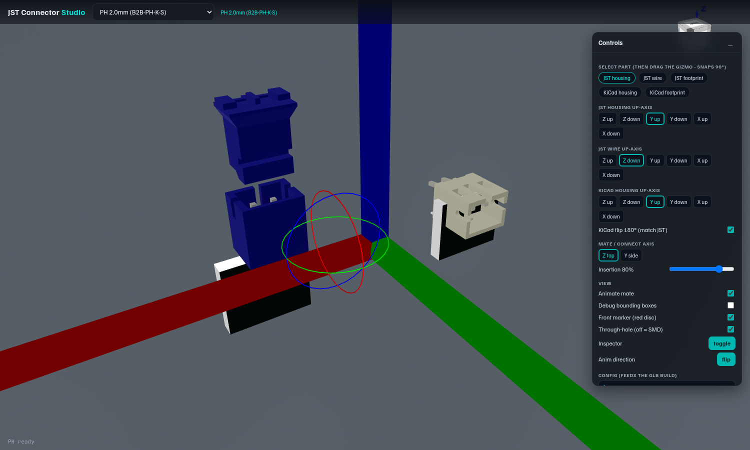
An interactive Babylon 9.5 studio for JST wire-to-board connectors. Load a system and see the
JST manufacturer housing + wire + ds2sf footprint mate in a looping animation, beside the
KiCad housing + footprint + silkscreen. Rotate every part with 90-degree-snap gizmos, set
mate axis / insertion / SMD-vs-THT / front-marker, toggle debug bounding boxes, and export a
config that drives the wiki component-page GLB build. AI-controllable (window.JSTStudio + /api).
Run it
adompkg install adom/jst-connector-cad   # installs the `jst-studio` command
jst-studio serve                         # http://localhost:8791
Open that URL in a Hydrogen webview panel. Built on adom-3d-viewer-babylon9 (Babylon 9.5 + Inspector).
JST connector CAD
Source JST connector CAD the manufacturer-first way and turn it into an interactive, animated, footprint-accurate wiki component page. The 3D model is JST's own STEP. KiCad is used only for the redistributable symbol and footprint, and as a side-by-side comparison foil. Built and verified end-to-end on five 2-circuit systems (PH, XH, SH, GH, ZH).
This README is the full illustrated walkthrough: what the pipeline does, how each decision was made, what gets published, how chip-fetcher and the KiCad references are used, and the viewer gotchas that cost real time. The installable recipe is in SKILL.md.
Why manufacturer-first: an engineer placing a JST part wants the real part. KiCad's generic 3D is fine for clearance, but the manufacturer STEP is the truth. So chip-fetcher always treats JST's STEP as the deliverable and KiCad as the comparison, never the reverse.
The pipeline at a glance
JST email-gated STEP ─┐
KiCad sym + fp + 3D ──┤→ STEP→GLB (decompress) → orient → compose scene → animate → publish
                      │     (step2glb)            (per part)   (trimesh)   (gltf-transform)  (adompkg)
service-kicad ────────┘
Every stage is numerically self-checked (bbox asserts) and visually verified by screenshotting the live Babylon viewer and reading it. matplotlib renders geometry but not textures or text, so it cannot be trusted for labels, footprints, or orientation.
1. Get the manufacturer CAD (email-gated)
JST gates STEP downloads behind a License Agreement email form on jst-mfg.com, and the USA
jst.com Cloudflare-walls headless browsers. So chip-fetcher drives the user's real browser
(native-browser bridge), fills the form, and retrieves the emailed STEP through the Gmail API
(adom-google). Rules learned the hard way: one submit per file, dedupe before sending, route to
a filtered alias, and trash demo emails afterward. The full flow lives in chip-fetcher playbooks
jst.md and jst-email-retrieval.md.
For each 2-circuit system you fetch three real parts: the board header, the wire housing, and the crimp contacts.
2. Look up the KiCad reference (symbol + footprint, and 3D if it exists)
service-kicad resolves the KiCad library footprint and symbol. The footprint is what makes the
3D scene honest: its pad coordinates are real millimetres.

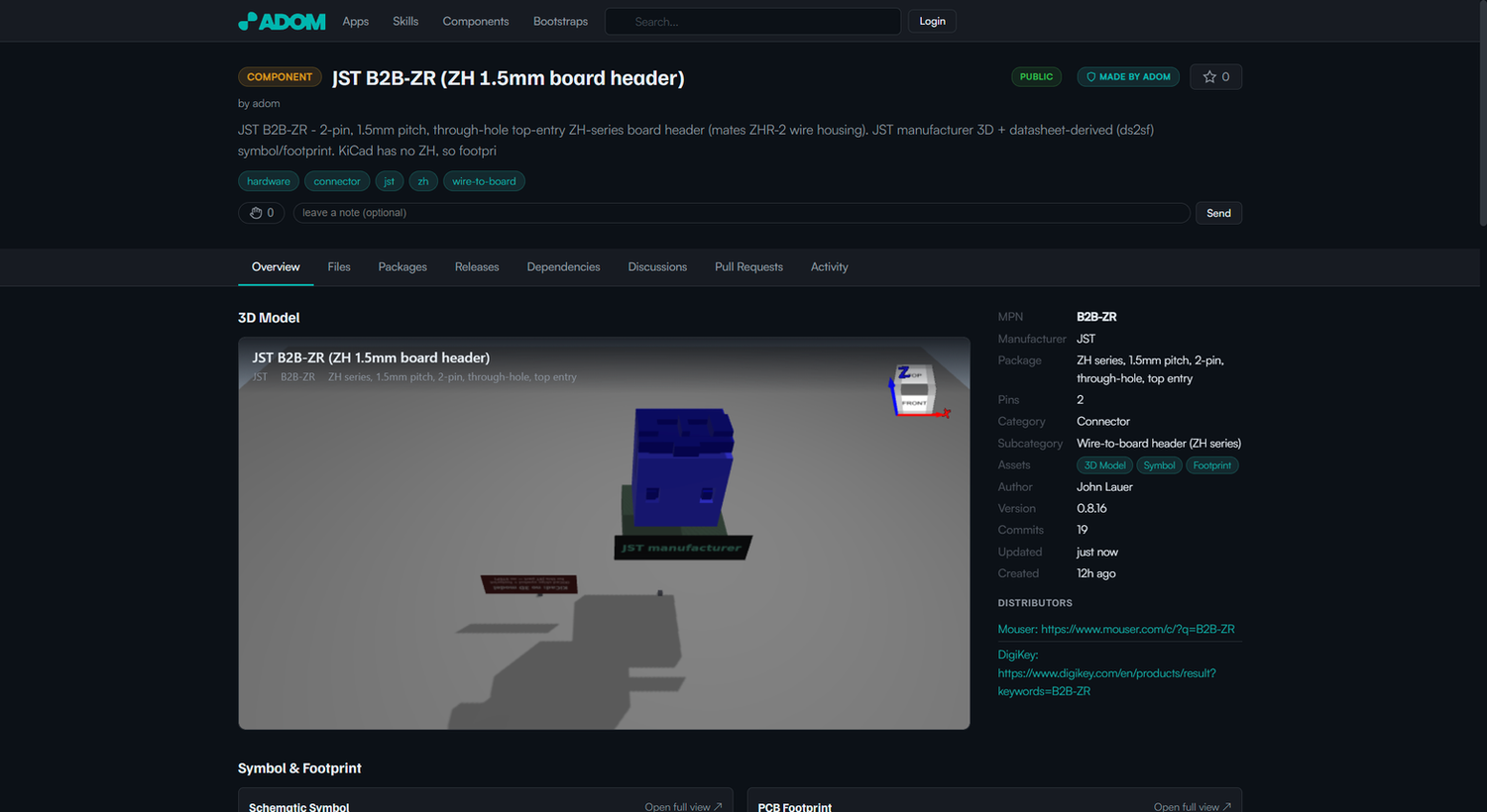
Not every JST part has a KiCad 3D model. ZH B2B-ZR returns 404 from kicad-packages3d, so its
page is single-column and says so (see the placard in section 7). KiCad still provides its
footprint and symbol, so the comparison is not lost.
3. STEP to GLB, and getting orientation right
step2glb convert turns each STEP into GLB. It emits Draco-compressed GLB that trimesh
cannot read, so it is decompressed first with @gltf-transform. Each model sits in its own
native frame, so orientation is read directly with step2glb thumbnail --pose front|top|side
(and features) rather than guessed from the bounding box (connectors are nearly cubic and fool
bbox heuristics). KiCad models are reliably Z-up with pins down; the JST THT boards here needed a
90 degree rotation about X.
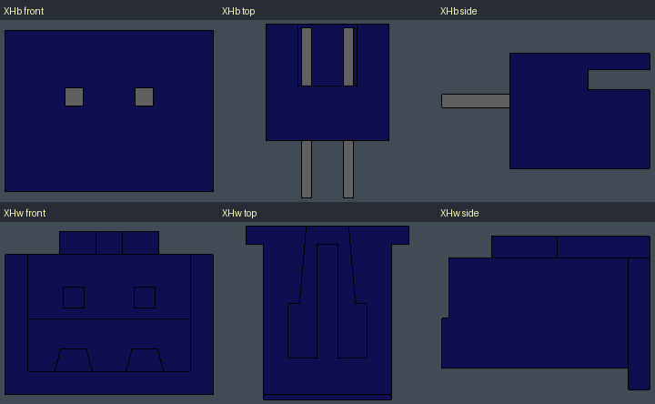
The part number encodes the mating axis: a B prefix (B2B, BM) is top entry (wire mates straight
down), an S prefix (SM, S2B) is side entry (wire mates horizontally).
4. Compose the scene (this is the part that matters)
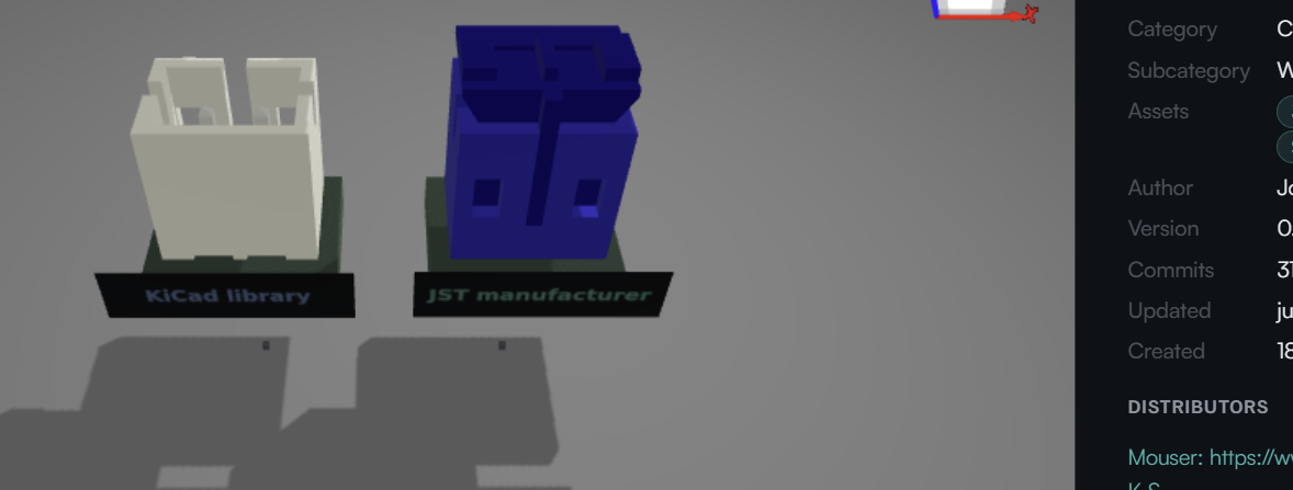
Two columns: KiCad foil on the left (tan), JST manufacturer on the right (blue). Then four things have to be exactly right, and each one was wrong at least once before it was right.
Seat the body, not the bounding box. The connector body bottom (where the cross-section
widens above the thin pins) sits on the PCB top. Seating by bbox.min sinks the housing into the
board. The body bottom is found by walking z-slices for the first wide slice.
True-scale footprint pads, registered to the real pins. The footprint is not a pasted image.
The .kicad_mod is parsed and copper pads are drawn at real millimetre coordinates, then
registered onto the connector's actual pin positions detected from the mesh. The build prints a
numeric check so a human can confirm alignment:
CHK board0 pins_through=True pin1=[1.95,-0.60] pin2=[3.95,-0.60] pad_pitch=2.0 pin_pitch=2.0
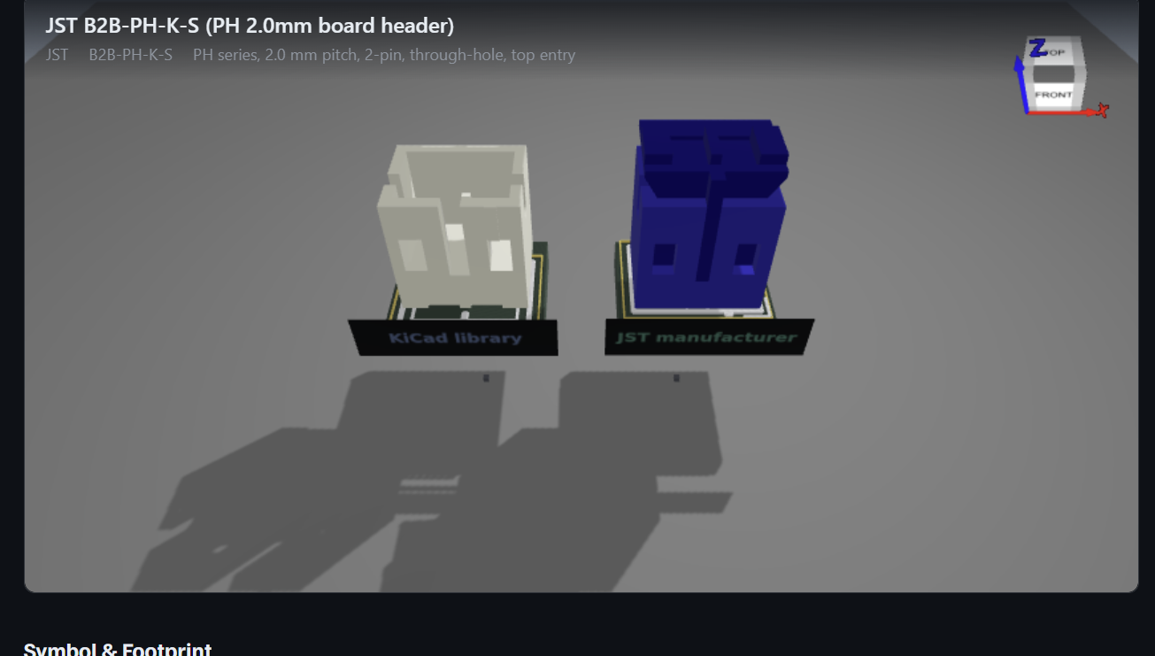
Silkscreen and courtyard. The silk outline (housing size) and courtyard (keep-out) are parsed
from the same .kicad_mod and drawn on the PCB with the same registration, so they sit correctly
around the part:
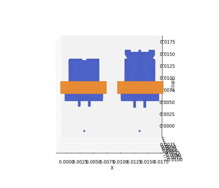
Float the PCB and show pins through. The PCB is a thin 1.6 mm slab floating about 8 mm up, with no riser (a riser hides the underside). THT pins pass through the slab and protrude out the bottom. A tiny invisible anchor at z=0 forces the viewer (which grounds to the lowest geometry) to put the floor low, so the camera can look under the PCB:
5. Animate the mate
The board and wire are given named nodes, baked at their seated pose (so a non-animating
viewer still looks right), then animated with @gltf-transform translation channels: the board
descends so the pins pass through, then the wire inserts about 80 percent into the board body so
the contact slots engage. Lifts are kept small and the loop dwells on the fully-mated state, which
is the shot that matters. The Babylon viewer autoplays and loops embedded GLB animations.
6. Viewer gotchas (verify, do not assume)
- Screenshot your own 3D view in the live viewer and read it. This is the single most important habit. matplotlib hides texture and text problems.
- The viewer is an iframe (
/viewer/3d/component/<slug>). Reloading the parent page does not refresh the iframe's cached GLB. Bump the GLB filename and bust the iframesrc. - Texture orientation: the quad UV needs
[[0,1],[1,1],[1,0],[0,0]]for upright, and Babylon flips U on the camera-facing face, so the image is pre-mirrored. Two-sided labels need separated single-winding quads backed opaque (coplanar faces z-fight, transparent PNGs bleed through). - KiCad models often sit 180 degrees about Z versus the manufacturer part, so the KiCad board gets a 180 degree Z rotation to match.
- Publish org-owned:
adompkg publish --org adom.
7. The five results
When KiCad has no 3D model, the column becomes a red placard so the absence is explained:
Live, animated component pages built with this exact pipeline:
- B2B-PH-K-S (PH 2.0 mm)
- B2B-XH-A (XH 2.5 mm)
- SM02B-SRSS-TB (SH 1.0 mm, side entry)
- BM02B-GHS-TBT (GH 1.25 mm SMT)
- B2B-ZR (ZH 1.5 mm, no KiCad 3D)
See also: chip-fetcher.