adom-layout-viewer
Public Made by Adomby adom
Interactive PCB layout viewer: your EDA's own render plus live net/trace highlighting and per-pad stock, price and wiki lookup
| Name | Last updated |
|---|---|
| bin | 1d ago |
| screenshots | 1d ago |
| scripts | 1d ago |
| src | 1d ago |
| .gitignore | 1d ago |
| build.sh | 1d ago |
| Cargo.lock | 1d ago |
| Cargo.toml | 1d ago |
| install.sh | 1d ago |
| LICENSE | 1d ago |
| package.json | 1d ago |
| page.json | 1d ago |
| README.md | 1d ago |
| release.sh | 1d ago |
| SKILL.md | 1d ago |
| uninstall.sh | 1d ago |
adom-layout-viewer
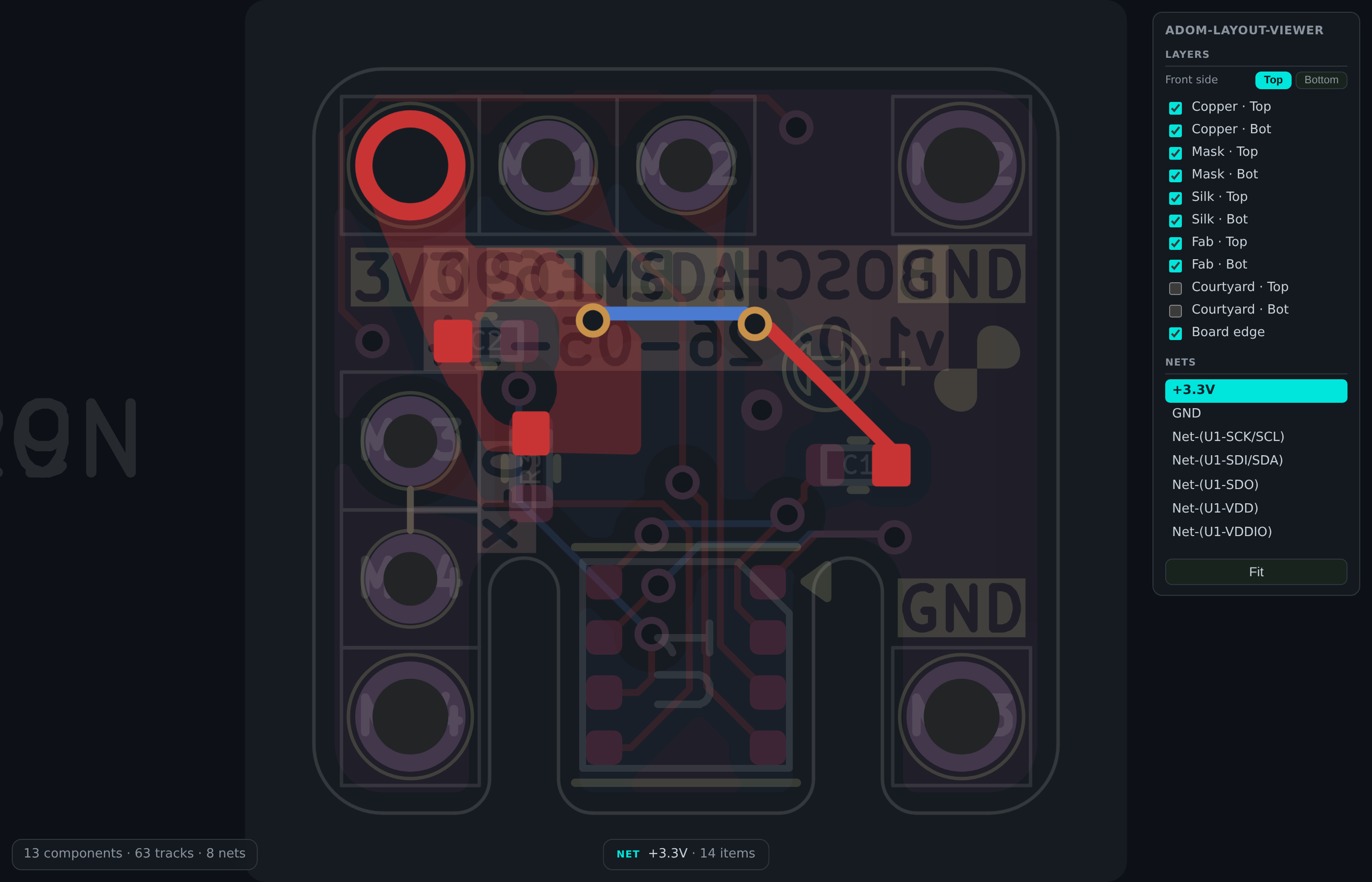
Interactive PCB layout viewer. The picture is your EDA's own export — the real silkscreen, the real trace widths, the real theme colours — and on top of it sits an invisible, coordinate-aligned interaction layer that knows the netlist. So you get a board that looks exactly like it does in KiCad, except you can click a pad and watch its entire net light up.
Why it works this way
A flat SVG export is authentic but dead — no nets, no pads, nothing to click. A self-drawn render is interactive but never quite looks like your EDA. This app does both at once:
- Visual base — per-layer SVG straight from the EDA (KiCad via the shared
service-kicad container,
POST /kicad/pcb/export/svg?layers=<L>), one group per layer, in KiCad's own theme colours. - Interaction overlay — the
.kicad_pcbparsed in Rust into pads, traces, vias and zones carryingdata-net/data-ref, drawn invisibly in the same board-mm coordinate system. No Y-flip, no offset, so the two align exactly.
What you get
Net highlighting — click any pad, via, trace or zone fill; the whole net lights in its own copper colour while the rest of the board dims. The net list on the right stays in sync (and is clickable itself).
Per-pad hover — pad number, size, shape, side and net, plus live stock, price, wiki page and popularity for the parent part.
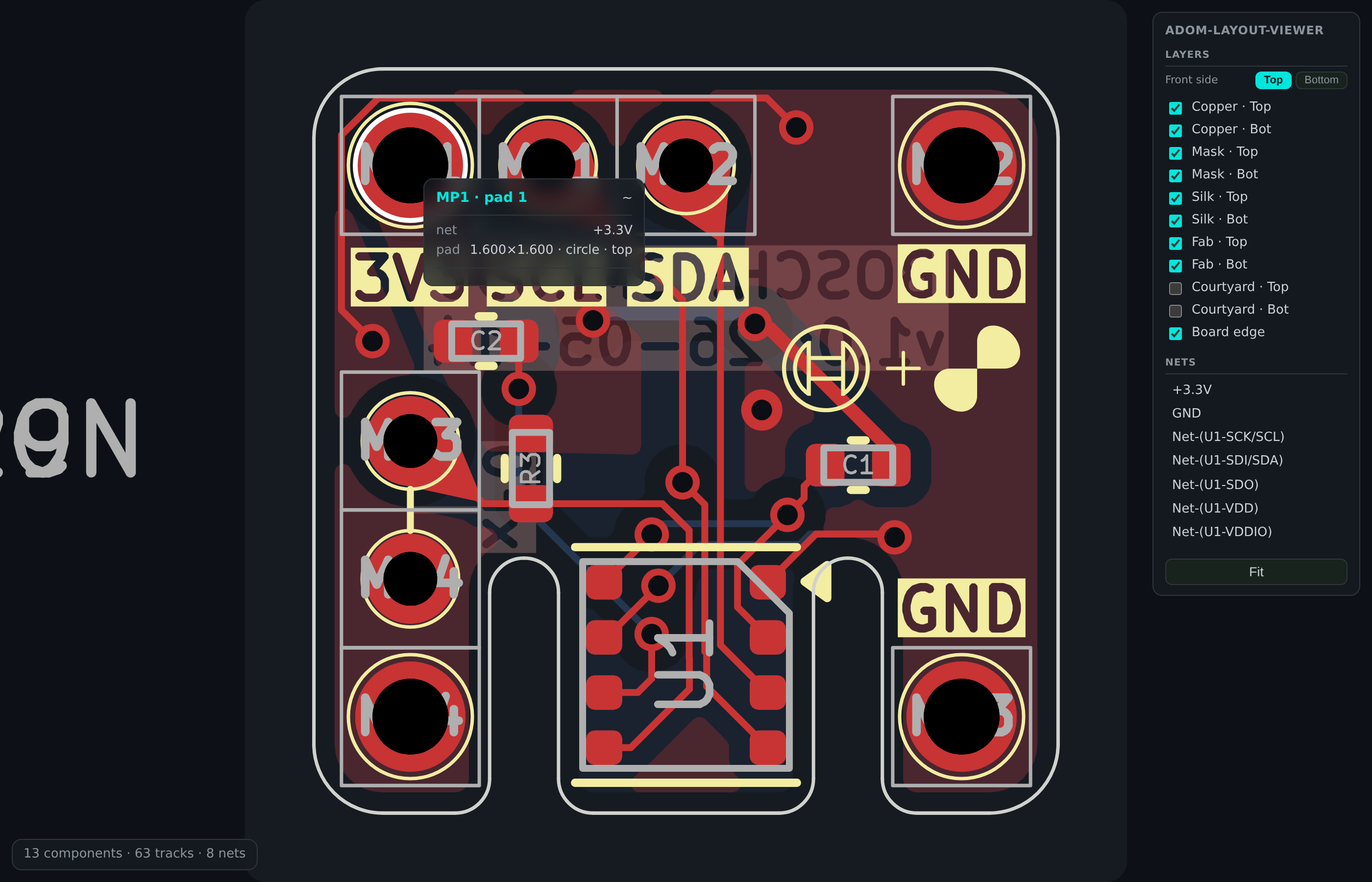
Layer control — every layer toggles independently, and the Top/Bottom switch mirrors the board and brings that side's stack to the front so you can select parts on the far side.
Embeddable —
embedemits one self-contained interactive HTML file with no external assets, so any app can drop it in an iframe as a live PCB view. (adom-project-manager uses exactly this for its board pane.)
Install
adompkg install adom-layout-viewer
Use
# one self-contained interactive HTML (what you embed in another app)
adom-layout-viewer embed --file board.kicad_pcb --out board.html

# a composed interactive SVG (+ board.meta.json with --meta)
adom-layout-viewer render --file board.kicad_pcb --out board.svg --meta

# the live app — hover/click, with enrichment served from /enrich
adom-layout-viewer serve --file board.kicad_pcb --port 8790
Embedding in your own app
embed inlines the SVG, the metadata and the viewer JS into a single file, so
an iframe is all you need:
<iframe src="/board-view/my-board/pcb" style="border:0;width:100%;height:100%"></iframe>
An embed has no server of its own, so its enrichment fetch("enrich") is
relative — it resolves against whatever serves the page. Host apps can
answer it (/…/enrich?mpn=&lcsc=) to give the embedded card live stock and
price; if nothing answers, the card simply shows identity only.
Enrichment
Hover data comes from sibling Adom CLIs, cached per part and fetched off the
render path (/enrich returns {"pending":true} and warms in the background,
so hovering never blocks):
adom-parts-search search <mpn>— stock and priceadom-wiki discover search --query <mpn> --json— wiki page and popularity
Notes
- Requires network access to service-kicad; override with
KICAD_SERVICE_API. If it is unreachable the app falls back to its own self-render so you still get a usable (if less authentic-looking) board. - KiCad today; the same overlay architecture is what will carry Altium and Fusion exports.
See also: adom-schematic-viewer — the same idea for .kicad_sch.