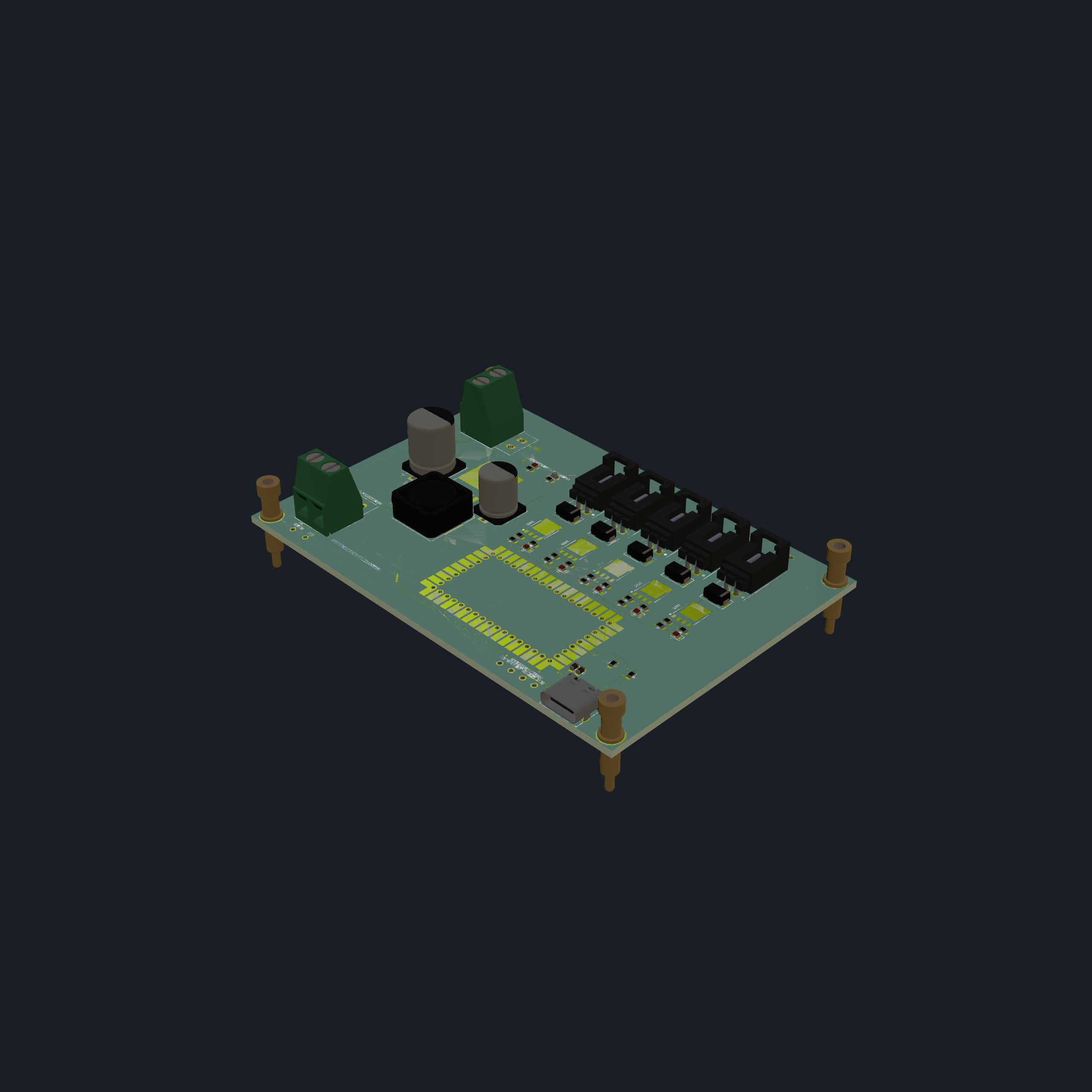
Teazzers Solenoid Driver RP2040 v1.1
Solenoid driver molecule for the Teazzers beverage dispensing workcell — 102.4×70.4 mm, 5-channel MOSFET driver with RP2040 PICAN castellated module (CAN FD + USB-C), 24V-to-5V buck regulator, and 29 machine contacts. Controls up to 5 solenoid valves and 1 pressure pump via individual high-side MOSFET switches.
Overview
| Property |
Value |
| Molecule ID |
teazzers-solenoid-driver-rp2040-v1-1 |
| Customer |
Teazzers |
| Board Size |
102.4 × 70.4 mm |
| MCU Module |
RP2040 PICAN Castellated v1 (U401) — RP2040 + MCP251863 CAN FD |
| MOSFET Drivers |
5× PSMN1R2-30YLD (LFPAK56) — low Rds(on) N-channel |
| Power Input |
24V DC via screw terminals |
| Regulator |
LM2596S-5 — 24V to 5V, 3A buck converter |
| USB |
USB-C 2.0 (UFP, 5.1k pull-down) for programming |
| Connectors |
Screw terminals (Phoenix/WAGO), JST-XH, Molex, pin headers |
| KiCad Version |
7/8 |
Sub-Modules
This molecule contains the RP2040 PICAN Castellated v1 as a soldered castellated sub-module (U401). For firmware development, programming, SWD debugging, USB bootloader usage, CAN bus configuration, and the full GPIO/SPI/I2C pinout of the MCU, refer to the PICAN module's wiki page. The PICAN provides the RP2040 MCU, MCP251863 CAN FD controller/transceiver, 16 MB QSPI flash, and USB-C connectivity.
Functional Blocks
5V Buck Regulator
- U201: LM2596S-5 — 24V input, 5V/3A output
- L201: SRR1260-470M (47 µH inductor)
- C202, C203: 220 µF electrolytic caps (input/output)
- D201: SS34 Schottky flyback diode
- Jumper JP201 selects power source: VBUS (USB), +5V_OUT (regulator), or +5V input
MCU — RP2040 PICAN Castellated Module
- U401: RP2040 PICAN Castellated v1 — soldered as a castellated sub-module
- Dual-core Arm Cortex-M0+ with integrated MCP251863 CAN FD controller/transceiver
- 16 MB QSPI flash, 12 MHz crystal
- USB-C routed through to J402 on the carrier board
- SWD debug pads (MC411/MC412) and BOOT/RST pads (MC413/MC414) on right edge
PICAN GPIO → Driver Function Mapping
MOSFET Gate Drives (solenoid switching)
| RP2040 GPIO |
PICAN Pad |
Driver Net |
Function |
| GPIO4 |
X9 |
/FET5_GATE |
Solenoid CH5 gate |
| GPIO5 |
X10 |
/FET4_GATE |
Solenoid CH4 gate |
| GPIO6 |
X11 |
/FET3_GATE |
Solenoid CH3 gate |
| GPIO7 |
X12 |
/FET2_GATE |
Solenoid CH2 gate |
| GPIO8 |
X13 |
/FET1_GATE |
Solenoid CH1 gate |
Pump Control
| RP2040 GPIO |
PICAN Pad |
Driver Net |
Function |
| GPIO11 |
X16 |
/PUMP1 |
Pump 1 control |
| GPIO12 |
X17 |
/PUMP2 |
Pump 2 control |
| GPIO13 |
X18 |
/PUMP3 |
Pump 3 control |
| GPIO14 |
X19 |
/PUMP4 |
Pump 4 control |
| GPIO15 |
X20 |
/PUMP5 |
Pump 5 control |
Status LEDs
| RP2040 GPIO |
PICAN Pad |
Driver Net |
Function |
| GPIO9 |
X14 |
/LED1 |
LED1 indicator |
| GPIO10 |
X15 |
/LED2 |
LED2 indicator |
| GPIO16 |
X21 |
/LED3 |
LED3 indicator |
| GPIO18 |
X38 |
/LED4 |
LED4 indicator |
Programming & Debug
| Signal |
PICAN Pad |
Driver Net |
Machine Contact |
| USB D+ |
X41 |
/USB_D+ |
MC402 |
| USB D- |
X40 |
/USB_D- |
MC403 |
| SWD_CLK |
X34 |
/SWD_CLK |
MC411 |
| SWD_IO |
X35 |
/SWD_IO |
MC412 |
| BOOT |
X36 |
/BOOT |
MC413 |
| RST |
X57 |
/RST |
MC414 |
Unused PICAN GPIOs
22 PICAN pads are not connected on the driver board:
| PICAN Pad |
GPIO / Function |
| X5 |
GPIO0 / UART0 TX |
| X6 |
GPIO1 / UART0 RX |
| X7 |
GPIO2 / I2C1 SDA |
| X8 |
GPIO3 / I2C1 SCL |
| X22 |
GPIO17 / LED data |
| X23 |
GPIO19 |
| X24–X27 |
GPIO20–23 / SPI (SDI, CS, SCK, SDO) |
| X29 |
GPIO25 |
| X30–X33 |
A0–A3 (GPIO26–29) / ADC |
| X37 |
GPIO24 |
| X42–X43 |
nINT1, nINT0/XSTBY (MCP251863) |
| X44, X53 |
RXD, TXD (MCP251863) |
| X47 |
nINT (MCP251863) |
| X54 |
STBY (MCP251863) |
| X55–X56 |
CANH, CANL (CAN bus) |
5-Channel MOSFET Driver
Each channel (Q301, Q503, Q601, Q701, Q801) is identical:
- PSMN1R2-30YLD N-channel MOSFET (30V, 1.2 mΩ Rds(on), LFPAK56)
- 24k gate pull-down resistor
- 10 Ω gate series resistor (current limiting)
- 10k pull-up for status feedback
- SS34 Schottky flyback diode per channel
- Red LED per channel for activity indication
Solenoid/Pump Outputs
| Channel |
Gate Net |
Drain Net |
Output Connector |
Function |
| 1 |
/FET1_GATE |
/DRAIN1 |
J301 + MC301/MC302 |
Solenoid 1 |
| 2 |
/FET2_GATE |
/DRAIN2 |
J502 + MC503/MC504 |
Solenoid 2 |
| 3 |
/FET3_GATE |
/DRAIN3 |
J601 + MC601/MC602 |
Solenoid 3 |
| 4 |
/FET4_GATE |
/DRAIN4 |
J701 + MC701/MC702 |
Solenoid 4 |
| 5 |
/FET5_GATE |
/DRAIN5 |
J801 + MC801/MC802 |
Solenoid 5 |
Each output pair has one drain contact and one +24V contact for the solenoid return path.
Machine Contact Pin Mapping
29 machine contacts across 3 edges.
Top Edge (Y = -1) — Signal & Control
| Contact |
Net |
Function |
| MC203 |
+5V_OUT |
5V regulated output |
| MC204 |
GND |
Ground |
| MC405 |
PUMP1 |
Pump control 1 |
| MC406 |
PUMP2 |
Pump control 2 |
| MC407 |
PUMP3 |
Pump control 3 |
| MC408 |
PUMP4 |
Pump control 4 |
| MC409 |
PUMP5 |
Pump control 5 |
| MC410 |
GND |
Ground |
| MC401 |
VBUS |
USB VBUS |
| MC402 |
USB_D+ |
USB data + |
| MC403 |
USB_D- |
USB data - |
| MC404 |
GND |
Ground |
Right Edge (X = 97) — Debug & Programming
| Contact |
Net |
Function |
| MC411 |
SWD_CLK |
SWD debug clock |
| MC412 |
SWD_IO |
SWD debug data |
| MC413 |
BOOT |
Bootloader select |
| MC414 |
RST |
Reset |
Left Edge — Power Input
| Contact |
Net |
Function |
| MC201 |
GND |
Ground |
| MC202 |
+24V |
24V power input |
Bottom Edge (Y = -65) — Solenoid Outputs
| Contact |
Net |
Function |
| MC301 |
DRAIN1 |
Solenoid 1 drain |
| MC302 |
+24V |
Solenoid 1 supply |
| MC503 |
DRAIN2 |
Solenoid 2 drain |
| MC504 |
+24V |
Solenoid 2 supply |
| MC601 |
DRAIN3 |
Solenoid 3 drain |
| MC602 |
+24V |
Solenoid 3 supply |
| MC701 |
DRAIN4 |
Solenoid 4 drain |
| MC702 |
+24V |
Solenoid 4 supply |
| MC801 |
DRAIN5 |
Solenoid 5 drain |
| MC802 |
+24V |
Solenoid 5 supply |
Connectors
| Ref |
Type |
Function |
| J201 |
Screw terminal (Phoenix, 5.00mm) |
24V power input |
| J202 |
Screw terminal (Phoenix, 5.00mm) |
5V power output |
| J203 |
Screw terminal (WAGO 2601, 3.50mm) |
24V power input (alt) |
| J204 |
Screw terminal (WAGO 2601, 3.50mm) |
5V power output (alt) |
| J205 |
Pin header 1×03 (2.54mm) |
Power source jumper |
| J301 |
Pin header 1×02 |
Solenoid 1 output |
| J401 |
JST-XH 1×06 (2.50mm) |
3.3V logic connector |
| J402 |
USB-C receptacle |
Programming / power (UFP) |
| J502–J801 |
Pin header 1×02 |
Solenoid 2–5 outputs |
Power Architecture
+24V input ──→ LM2596S-5 ──→ +5V (3A)
                                  │
                        JP201 selects: VBUS / +5V_OUT / +5V
                                  │
                                  ▼
                        RP2040 PICAN module (internal 3.3V LDO)
Status LEDs
| LED |
Color |
Function |
| D202 |
Yellow |
24V power indicator |
| D203 |
Red |
Fault indicator |
| D401 |
Yellow |
5V power indicator |
| D402 |
Green |
MCU status |
| D403 |
Yellow |
CAN activity |
| D404 |
Green |
USB activity |
| LED301, LED502, LED601, LED701 |
Red |
Per-channel solenoid activity |
Fabrication
- BOM:
jlcpcb/production_files/BOM-Taprite-MOSFET-board-as-molecule_rework_PICAN_v1.csv
- CPL:
jlcpcb/production_files/CPL-Taprite-MOSFET-board-as-molecule_rework_PICAN_v1.csv
- Gerbers:
jlcpcb/production_files/GERBER-Taprite-MOSFET-board-as-molecule_rework_PICAN_v1.zip
3D Models
Teazzers_Solenoid_Driver_RP2040_v1.1.glb — assembled board with PICAN module (5.1 MB)Taprite-MOSFET-board-as-molecule_rework_v1-1.glb — board-only variant (6.0 MB)