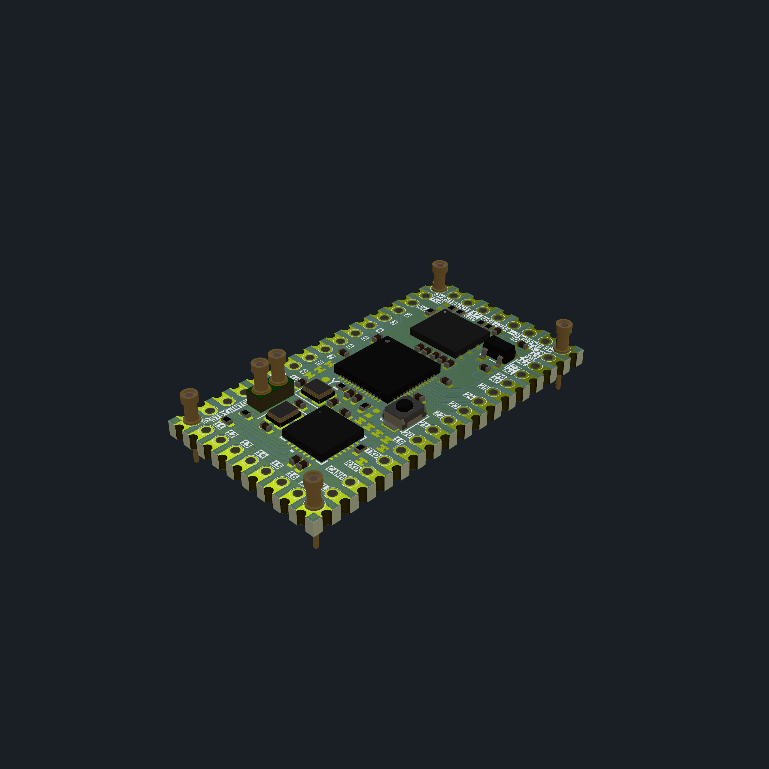
RP2040 PICAN Castellated Molecule v1
Castellated RP2040 molecule with integrated MCP251863 CAN bus controller/transceiver — 19×35 mm, 4 corner machine pins, 49 castellated machine contacts. USB-C, 16 MB QSPI flash, SWD debug, and 120 Ω CAN termination on-board.
Overview
| Property |
Value |
| Molecule ID |
rp2040-pican-castellated-v1 |
| Board Size |
19.0 × 35.0 mm |
| Layers |
2 |
| MCU |
RP2040 (Raspberry Pi, QFN-56) |
| CAN Controller |
MCP251863T-E/9PX (Microchip, integrated CAN FD controller + transceiver) |
| Flash |
W25Q128JVPIQ — 16 MB QSPI |
| Regulator |
AP2112K-3.3 (3.3V LDO from 5V input) |
| USB |
USB-C 2.0 with USBLC6-2P6 ESD protection |
| Crystal |
12 MHz (RP2040), 40 MHz (MCP251863) |
| Castellated Pads |
49 machine contacts + 4 corner machine pins |
| KiCad Version |
7/8 |
Key ICs
| Ref |
Part |
Package |
Function |
| U4 |
RP2040 |
QFN-56 |
Dual-core Arm Cortex-M0+ MCU |
| U2 |
MCP251863T-E/9PX |
VQFN-28 |
CAN FD controller + transceiver (SPI interface) |
| U3 |
W25Q128JVPIQ |
WSON-8 |
16 MB QSPI flash |
| U6 |
AP2112K-3.3 |
SOT-23-5 |
3.3V 600mA LDO regulator |
| U1 |
USBLC6-2P6 |
SOT-23-6 |
USB ESD protection |
| U5 |
74LVC1T45 |
SOT-23-5 |
Level translator (LED data) |
Machine Contact Pin Mapping
4 corner machine pins (X1–X4) for power/ground, 49 castellated contacts for signals.
Corner Machine Pins
| Pin |
Position |
Net |
Function |
| X1 |
Bottom-left (1, 7) |
GND |
Ground |
| X2 |
Top-left (1, -25) |
+3V3 |
3.3V output |
| X3 |
Top-right (17, -25) |
+5V |
5V input |
| X4 |
Bottom-right (17, 7) |
GND |
Ground |
Left Edge Contacts (bottom to top)
| Contact |
Net |
Function |
| X54 |
STBY |
CAN standby control |
| X43 |
nINT0/GPIO0/XSTBY |
CAN interrupt 0 / GPIO0 |
| X42 |
nINT1/GPIO1 |
CAN interrupt 1 / GPIO1 |
| X47 |
nINT |
CAN interrupt |
| X15 |
GPIO10 |
General purpose I/O |
| X14 |
GPIO9 |
General purpose I/O |
| X13 |
GPIO8 |
General purpose I/O |
| X12 |
GPIO7 |
General purpose I/O |
| X11 |
GPIO6 |
General purpose I/O |
| X10 |
GPIO5 |
General purpose I/O |
| X9 |
GPIO4 |
General purpose I/O |
| X8 |
GPIO3 / SCL1 |
I2C1 clock |
| X7 |
GPIO2 / SDA1 |
I2C1 data |
| X6 |
GPIO1 / RX0 |
UART0 RX |
| X5 |
GPIO0 / TX0 |
UART0 TX |
Right Edge Contacts (bottom to top)
| Contact |
Net |
Function |
| X56 |
CANL |
CAN Low bus line |
| X55 |
CANH |
CAN High bus line |
| X44 |
RXD |
CAN RX data |
| X53 |
TXD |
CAN TX data |
| X23 |
GPIO19 |
General purpose I/O |
| X24 |
GPIO20 / SDI |
SPI data in |
| X25 |
GPIO21 / CS |
SPI chip select |
| X26 |
GPIO22 / SCK |
SPI clock |
| X27 |
GPIO23 / SDO |
SPI data out |
| X37 |
GPIO24 |
General purpose I/O |
| X29 |
GPIO25 |
General purpose I/O |
| X30 |
A0 (GPIO26) |
ADC channel 0 |
| X31 |
A1 (GPIO27) |
ADC channel 1 |
| X32 |
A2 (GPIO28) |
ADC channel 2 |
| X33 |
A3 (GPIO29) |
ADC channel 3 |
Top Edge Contacts (left to right)
| Contact |
Net |
Function |
| X57 |
RST |
Reset |
| X36 |
BOOT |
Bootloader select |
| X22 |
GPIO17 / LED |
User LED data line |
| X41 |
USB+ |
USB data positive |
| X40 |
USB- |
USB data negative |
| X35 |
SWD_IO |
SWD debug data |
| X34 |
SWD_CLK |
SWD debug clock |
Bottom Edge Contacts (left to right)
| Contact |
Net |
Function |
| X16 |
GPIO11 |
General purpose I/O |
| X17 |
GPIO12 |
General purpose I/O |
| X18 |
GPIO13 |
General purpose I/O |
| X19 |
GPIO14 |
General purpose I/O |
| X20 |
GPIO15 |
General purpose I/O |
| X21 |
GPIO16 |
General purpose I/O |
| X38 |
GPIO18 |
General purpose I/O |
CAN Bus Interface
The MCP251863T provides integrated CAN FD controller and transceiver connected to the RP2040 via SPI. Features:
- CAN 2.0B and CAN FD support
- On-board 120 Ω termination resistor (R20, solder jumper configurable)
- CANH/CANL brought out to castellated pads X55/X56
- 40 MHz crystal (Y2)
- Interrupt lines (nINT, nINT0, nINT1) exposed on left edge
Power
| Rail |
Source |
Regulator |
| +5V |
USB-C or X3 corner pin |
Input rail |
| +3V3 |
AP2112K-3.3 LDO from 5V |
Powers RP2040, flash, CAN controller |
| +1V1 |
RP2040 internal |
Core voltage |
500 mA polyfuse (F1) on USB input. Schottky diode (D3, PMEG2010BELD) for reverse protection.
Solder Jumpers
| Jumper |
Default |
Function |
| JP1 |
Open |
USB VBUS select |
| JP2 |
Bridged 1-2 |
Power source select |
| JP3 |
Open |
CAN termination enable |
| JP4–JP9 |
Bridged |
GPIO routing configuration |
| JP10–JP12 |
Bridged |
CAN signal routing |
Debug & Programming
- USB-C: Native USB bootloader (hold BOOT + reset)
- SWD: Test points TP1 (CLK) and TP2 (DIO), also on castellated pads X34/X35
- BOOT button: SW1
- Reset button: SW2
Fabrication
- Gerber files:
jlcpcb/gerber/
- Production files:
jlcpcb/production_files/
Issues
- No GLB 3D model included in the project —
packages3D_incomplete/ contains individual component models but no assembled board model
- Lock files present (
~*.lck) suggest the project may have been exported while open in KiCad