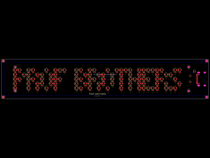
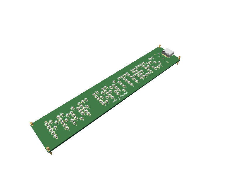
component
Prof Brothers LED Nameplate
Unreviewed136x24mm USB-C desk nameplate with 117 white LEDs spelling PROF BROTHERS in a 3x5 pixel font. Georgia Tech. Plug in any iPhone charger and it lights up.
3D Model
Symbol & Footprint
Schematic

PCB Footprint
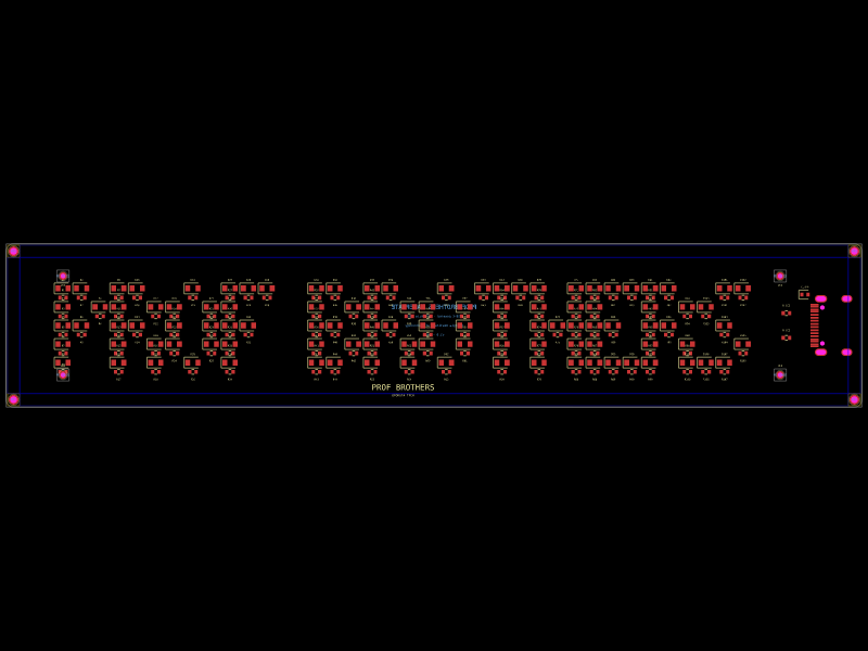
Overview
A white LED desk nameplate that spells PROF BROTHERS in a 3x5 bitmap pixel font. Designed as an Adom molecule (136 x 24 mm, 4-pin machine contact) so it can be manufactured on the InstaPCB workcell. Built for Prof Tim Brothers at Georgia Institute of Technology.
How it works
- 117 white LEDs (0603) arranged in 13 letters: P-R-O-F B-R-O-T-H-E-R-S
- Each LED has its own 220 ohm current-limiting resistor (0402)
- All LED+resistor pairs wired in parallel from VBUS to GND
- USB-C connector on the east edge with 5.1k ohm CC pull-downs
- 100nF bypass cap on VBUS for decoupling
- Total draw: ~1W at 5V, any phone charger handles it
How to use it
- Grab any USB-C cable (iPhone charger works)
- Plug one end into the board's east edge
- Plug the other end into a 5V USB-C power source
- PROF BROTHERS lights up white
Hardware summary
| Component | Value | Package | Qty |
|---|---|---|---|
| LED | white | 0603 | 117 |
| R | 220 ohm | 0402 | 117 |
| R_CC1, R_CC2 | 5.1k ohm | 0402 | 2 |
| C_BYP | 100nF | 0402 | 1 |
| J1 | TYPE-C-31-M-12 | USB-C | 1 |
Design details
- Board: 136 x 24 mm, 2-layer, 1.6mm FR4, round edges
- Molecule type: 4-pin with MachinePinMediumStandard
- 4 corner machine contacts: MC_VCC1/MC_VCC2 (north), MC_GND1/MC_GND2 (south)
- Pixel pitch: 3mm LED-to-LED, 3mm letter gap, 5mm word gap
- White LED Vf ~3.0V, so 220 ohm at 5V gives ~9mA per LED
- USB-C on east edge using UsbCReceptacle wrapper (TYPE-C-31-M-12, JLCPCB C165948)
- InstaPCB quote: $13.04/board (fab $2 + assembly $11.04)
Build commands
cd ~/project/adom-tsci/examples/ProfBrothers-Nameplate
bun install
bunx tsci build lib/index.tsx --glbs --svgs --3d-png --pcb-png
adom-tsci start .
Files attached
Source (recreate the molecule)
- plan.md - Original design brief and hardware decisions
- profbrothers-led-nameplate-source.tar.gz - Full tscircuit project (lib/, package.json, walkthrough.json). Untar and
bun install && bunx tsci buildto recreate.
Build outputs
- 3d.glb - Full 3D model, opens in any glTF viewer
- pcb.svg / schematic.svg - Vector PCB layout and schematic
- 3d.png / pcb.png - Raster previews
Fabrication files
- ProfBrothers-Nameplate-3d.kicad_pcb - KiCad PCB with all 226 3D model references injected and the USB-C footprint replaced with chip-fetcher's validated TYPE-C-31-M-12 pair. Open in KiCad, run DRC, export gerbers, or send directly to fab.
- gerbers.zip - Fab-ready gerber package: F_Cu, B_Cu, F_Mask, B_Mask, F_SilkScreen, B_SilkScreen, F_Paste, B_Paste, Edge_Cuts, drill files, BOM, and pick-and-place CSV. Upload directly to JLCPCB or hand to InstaPCB.
Built with
Authored in tscircuit (TSX), previewed with adom-tsci, validated in KiCad 3D viewer, published to the Adom Wiki. Georgia Institute of Technology.