iCE40HX1K — 1.28K-Cell Low-Power Non-Volatile FPGA
UnreviewedLattice iCE40HX1K — 1,280-cell ultra-low-power FPGA. Three matched symbol+footprint pairs with clean custom-rendered PNGs, interactive viewers, per-artifact provenance.
Symbol & Footprint
Schematic Symbol

Source: Lattice Semiconductor — iCE40 LP/HX Family Data Sheet (FPGA-DS-02029-4.1)
Manufacturer: Lattice Semiconductor
Part Number: iCE40HX1K
Document: FPGA-DS-02029-4.1 — Rev 4.1, April 2023 (53 pages)
Community Pinout Source: Project IceStorm — icebox/icebox.py (bitstream-verified I/O pin locations)
Description
Evidence: datasheet pages 8–10 — "General Description" section and Figure 3.1 iCE40LP/HX1K Device Top View.
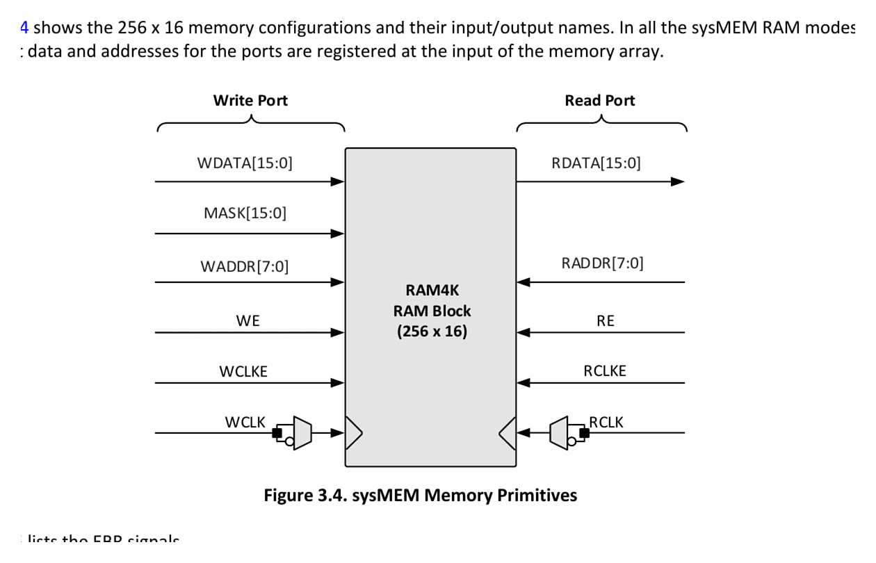
The iCE40HX1K is a member of the Lattice iCE40 LP/HX Family of ultra-low-power, non-volatile FPGAs. The HX series targets high-performance applications, while sharing the same 40 nm fabric and footprint-compatible package options as the LP series. The HX1K provides 1,280 logic cells, 64 Kbit of embedded block RAM, one PLL, and up to 95 user I/Os across four independently powered I/O banks.
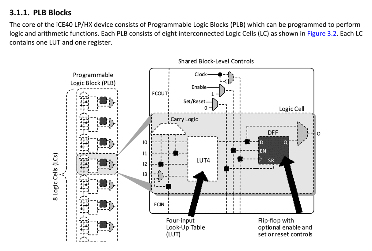
The fabric is based on Programmable Logic Blocks (PLBs), each consisting of eight Logic Cells. Every Logic Cell contains a 4-input LUT, a D-type flip-flop with programmable clock enable and set/reset, and dedicated carry logic. PLBs are connected through a row/column interconnect and can also be mapped as distributed memory. Configuration is loaded from an internal SRAM bitstream at power-up, driven either by a Master/Slave SPI flash or by the on-chip Non-Volatile Configuration Memory (NVCM).
Key Specifications
Evidence: datasheet page 9 Table 2.1 "iCE40 LP/HX Family Selection Guide" (HX1K column), page 21 Table 4.2 "Recommended Operating Conditions", page 33 Table 4.26 "External Switching Characteristics – HX Devices".
| Parameter | Value |
|---|---|
| Logic Cells (LUT4 + FF) | 1,280 |
| Embedded Block RAM (4-kbit blocks) | 16 (64 Kbit) |
| Phase-Locked Loops | 1 |
| Maximum User I/O | 95 |
| Maximum Differential Input Pairs | 12 |
| Core Supply Voltage (VCC) | 1.14 V – 1.26 V (1.2 V typ) |
| I/O Supply Range (VCCIO) | 1.71 V – 3.46 V |
| Global Clock fMAX (typ) | 275 MHz |
| Register-to-Register 16-bit counter | 255 MHz |
| 256 × 16 Dual-Port BRAM fMAX | 403 MHz |
| Static VCC Current (typ) | 296 µA |
| Junction Temperature (Industrial) | -40 °C to 100 °C |
| Process | 40 nm CMOS |
| Configuration | SPI Master/Slave, internal NVCM |
Features
Evidence: datasheet page 8 "Features" bullet list.
- Flexible logic architecture with 1,280 LUT4+FF logic cells
- 64 Kbit of sysMEM Embedded Block RAM (16 × 4-kbit EBRs), cascadable
- One sysCLOCK Phase-Locked Loop (PLL) with dynamic phase/delay adjustment
- Ultra-low-power 40 nm process; sub-µA standby modes
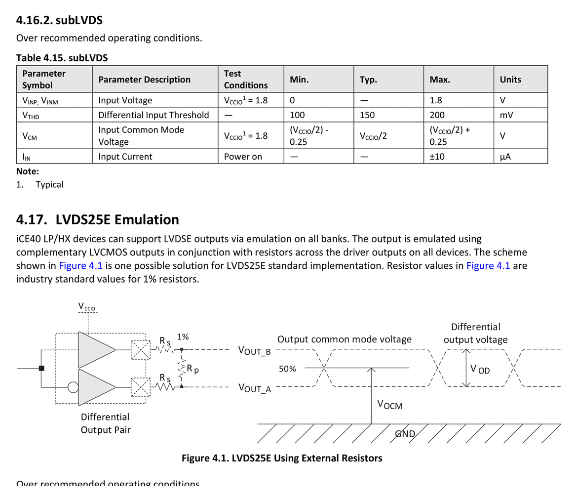
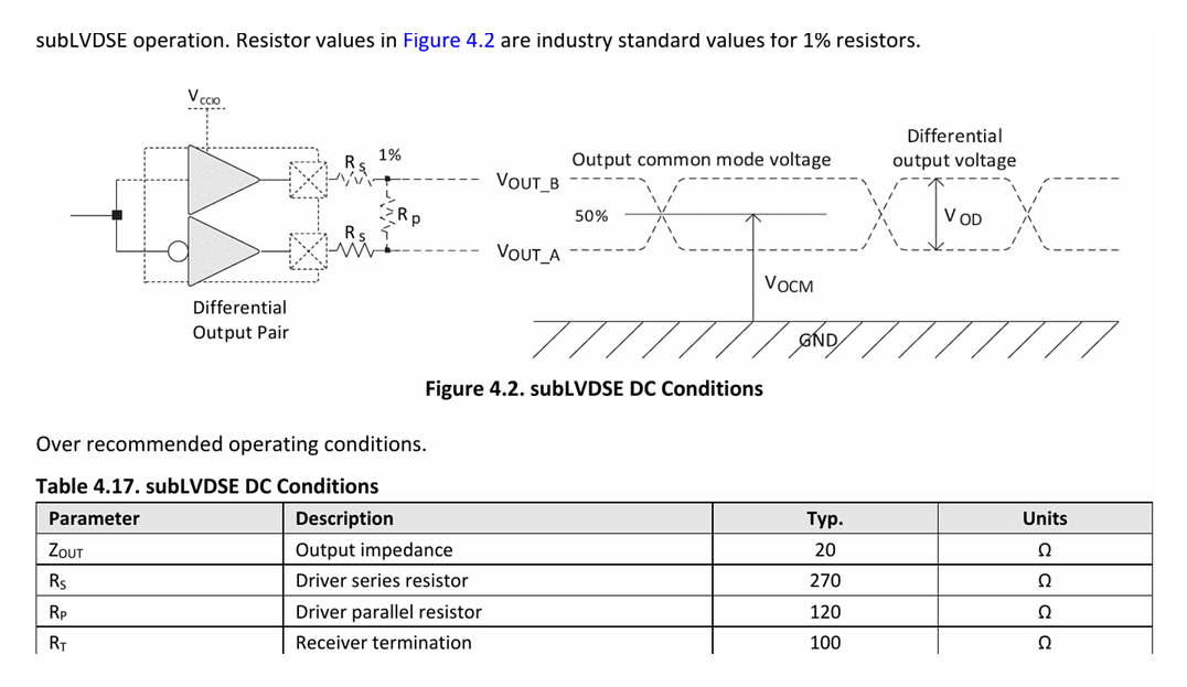
- Low-swing differential I/O: LVDS25 and subLVDS (emulated with external resistors)
- Broad single-ended I/O support: LVCMOS 3.3 / 2.5 / 1.8 / 1.5 / 1.2 V
- Schmitt-trigger inputs with 200 mV typical hysteresis, programmable pull-ups
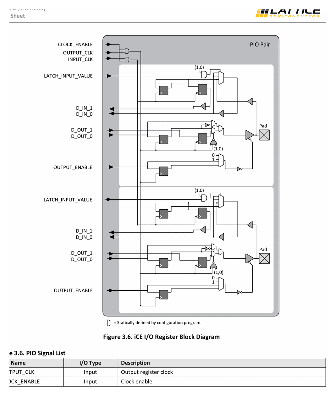
- Pre-engineered source-synchronous I/O with DDR registers in every PIO cell
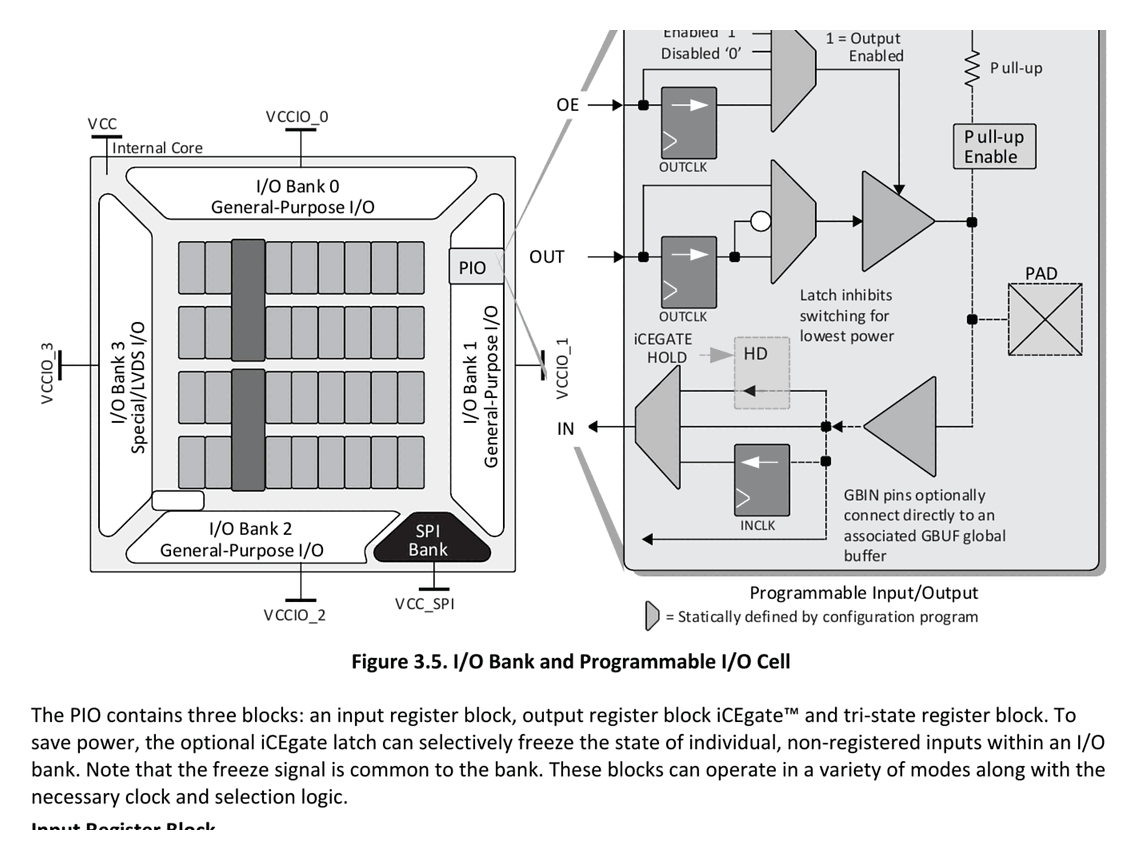
- Up to four independently powered I/O banks (VCCIO_0..3)
- Internal Non-Volatile Configuration Memory (NVCM) — no external boot flash required
- Configuration sources: Master SPI flash, Slave SPI, or internal NVCM (cold boot or warm boot)
- Package options: VQFP-100 (14 × 14 mm), caBGA-132 (8 × 8 mm, 0.5 mm pitch), TQFP-144 (20 × 20 mm)
- Halogen-free, RoHS-compliant; industrial temperature grade
Pin Configuration
Evidence: datasheet pages 38–42 — "Pinout Information" chapter. Per-ball pin signal names are sourced from Project IceStorm icebox/icebox.py (community-verified via bitstream fuzzing of real parts). Non-I/O pin positions (power, GND, config) require cross-reference with the Lattice per-package pinout CSV referenced on datasheet page 46 ("For Further Information → iCE40 Pinout Files").
Signal Naming Convention
General-purpose I/O pins are named IO[Bank]_[Row/Column][A/B], where [A] indicates the positive half of an LVDS pair and [B] the negative half. Signal names in the tables below use the IceStorm-encoded form IOB_<bank>_<x><y><A|B> where x,y is the chip-internal tile coordinate.
Dedicated Signal Pins
| Pin Name | Direction | Description |
|---|---|---|
| CRESET_B | Input | Active-low configuration reset (pulls CDONE low, restarts config) |
| CDONE | I/O | Configuration done — open-drain output; pulled high at end of config |
| CBSEL[0:1] | Input | Configuration boot select (ColdBoot/WarmBoot selection) |
| SPI_SCK | I/O | SPI configuration clock (Master or Slave mode) |
| SPI_SS | I/O | SPI chip-select; low during configuration |
| SPI_SI | I/O | SPI serial input / MOSI |
| SPI_SO | I/O | SPI serial output / MISO |
| GBIN[0:7] | Input | Global buffer input (dual-use with general I/O) |
Power Pins
| Pin Name | Typical Voltage | Description |
|---|---|---|
| VCC | 1.14 – 1.26 V | Core fabric supply (multiple pins, decoupled separately) |
| VCCIO_0 | 1.2 / 1.5 / 1.8 / 2.5 / 3.3 V | I/O bank 0 supply (top edge) |
| VCCIO_1 | 1.2 / 1.5 / 1.8 / 2.5 / 3.3 V | I/O bank 1 supply (right edge) |
| VCCIO_2 | 1.2 / 1.5 / 1.8 / 2.5 / 3.3 V | I/O bank 2 supply (bottom edge, shared with SPI) |
| VCCIO_3 | 1.2 / 1.5 / 1.8 / 2.5 / 3.3 V | I/O bank 3 supply (left edge) |
| VCCPLL | 1.14 – 1.26 V | Dedicated PLL supply (filter separately) |
| VCC_SPI | 1.71 – 3.46 V | SPI bank power (typically tied to VCCIO_2) |
| VPP_2V5 | 2.30 – 3.46 V (prog only) | NVCM programming supply; leave floating in applications |
| GND | 0 V | Ground reference (multiple pins) |
Package / I/O Summary — HX1K
Evidence: datasheet pages 41–42 "Pin Information Summary" columns for iCE40HX1K.
| Package | User I/O | LVDS Pairs | Bonded Pads | Body Size | Pitch |
|---|---|---|---|---|---|
| VQ100 (VQFP-100) | 72 | 9 | 100 | 14 × 14 mm | 0.5 mm |
| CB132 (caBGA-132) | 95 | 12 | 132 | 8 × 8 mm | 0.5 mm |
| TQ144 (TQFP-144) | 96 | 12 | 144 | 20 × 20 mm | 0.5 mm |
The full per-pin I/O assignments for each package are listed below, sourced from Project IceStorm's community-verified chip database (icebox/icebox.py in YosysHQ/icestorm). Non-I/O pin positions (VCC, GND, VCCIO_x, SPI_xxx, CRESET_B, CDONE) are not reproduced here — refer to the Lattice per-package pinout CSV linked on datasheet page 46 for authoritative mapping.
VQ100 — I/O Pin Assignments
Source: Project IceStorm icebox/icebox.py pin-location database (community-verified from bitstream fuzzing). 72 user I/O pins.
| Pin | Bank | Signal | Notes |
|---|---|---|---|
| 1 | 3 | IOB_3_0014B | tile (x=0, y=14, half=1) |
| 2 | 3 | IOB_3_0014A | tile (x=0, y=14, half=0) |
| 3 | 3 | IOB_3_0013B | tile (x=0, y=13, half=1) |
| 4 | 3 | IOB_3_0013A | tile (x=0, y=13, half=0) |
| 7 | 3 | IOB_3_0012B | tile (x=0, y=12, half=1) |
| 8 | 3 | IOB_3_0012A | tile (x=0, y=12, half=0) |
| 9 | 3 | IOB_3_0010B | tile (x=0, y=10, half=1) |
| 10 | 3 | IOB_3_0010A | tile (x=0, y=10, half=0) |
| 12 | 3 | IOB_3_0009B | tile (x=0, y=9, half=1) |
| 13 | 3 | IOB_3_0009A | tile (x=0, y=9, half=0) |
| 15 | 3 | IOB_3_0008B | tile (x=0, y=8, half=1) |
| 16 | 3 | IOB_3_0008A | tile (x=0, y=8, half=0) |
| 18 | 3 | IOB_3_0006B | tile (x=0, y=6, half=1) |
| 19 | 3 | IOB_3_0006A | tile (x=0, y=6, half=0) |
| 20 | 3 | IOB_3_0004B | tile (x=0, y=4, half=1) |
| 21 | 3 | IOB_3_0004A | tile (x=0, y=4, half=0) |
| 24 | 3 | IOB_3_0002B | tile (x=0, y=2, half=1) |
| 25 | 3 | IOB_3_0002A | tile (x=0, y=2, half=0) |
| 26 | 2 | IOB_2_0200A | tile (x=2, y=0, half=0) |
| 27 | 2 | IOB_2_0200B | tile (x=2, y=0, half=1) |
| 28 | 2 | IOB_2_0300A | tile (x=3, y=0, half=0) |
| 29 | 2 | IOB_2_0300B | tile (x=3, y=0, half=1) |
| 30 | 2 | IOB_2_0400A | tile (x=4, y=0, half=0) |
| 33 | 2 | IOB_2_0600B | tile (x=6, y=0, half=1) |
| 34 | 2 | IOB_2_0700A | tile (x=7, y=0, half=0) |
| 36 | 2 | IOB_2_0600A | tile (x=6, y=0, half=0) |
| 37 | 2 | IOB_2_0700B | tile (x=7, y=0, half=1) |
| 40 | 2 | IOB_2_0900B | tile (x=9, y=0, half=1) |
| 41 | 2 | IOB_2_1000A | tile (x=10, y=0, half=0) |
| 42 | 2 | IOB_2_1000B | tile (x=10, y=0, half=1) |
| 45 | 2 | IOB_2_1100A | tile (x=11, y=0, half=0) |
| 46 | 2 | IOB_2_1100B | tile (x=11, y=0, half=1) |
| 48 | 2 | IOB_2_1200A | tile (x=12, y=0, half=0) |
| 49 | 2 | IOB_2_1200B | tile (x=12, y=0, half=1) |
| 51 | 1 | IOB_1_1303B | tile (x=13, y=3, half=1) |
| 52 | 1 | IOB_1_1304A | tile (x=13, y=4, half=0) |
| 53 | 1 | IOB_1_1304B | tile (x=13, y=4, half=1) |
| 54 | 1 | IOB_1_1306A | tile (x=13, y=6, half=0) |
| 56 | 1 | IOB_1_1306B | tile (x=13, y=6, half=1) |
| 57 | 1 | IOB_1_1307A | tile (x=13, y=7, half=0) |
| 59 | 1 | IOB_1_1307B | tile (x=13, y=7, half=1) |
| 60 | 1 | IOB_1_1308A | tile (x=13, y=8, half=0) |
| 62 | 1 | IOB_1_1308B | tile (x=13, y=8, half=1) |
| 63 | 1 | IOB_1_1309A | tile (x=13, y=9, half=0) |
| 64 | 1 | IOB_1_1311A | tile (x=13, y=11, half=0) |
| 65 | 1 | IOB_1_1311B | tile (x=13, y=11, half=1) |
| 66 | 1 | IOB_1_1312A | tile (x=13, y=12, half=0) |
| 68 | 1 | IOB_1_1313A | tile (x=13, y=13, half=0) |
| 69 | 1 | IOB_1_1313B | tile (x=13, y=13, half=1) |
| 71 | 1 | IOB_1_1314A | tile (x=13, y=14, half=0) |
| 72 | 1 | IOB_1_1314B | tile (x=13, y=14, half=1) |
| 73 | 1 | IOB_1_1315A | tile (x=13, y=15, half=0) |
| 74 | 1 | IOB_1_1315B | tile (x=13, y=15, half=1) |
| 78 | 0 | IOB_0_1217B | tile (x=12, y=17, half=1) |
| 79 | 0 | IOB_0_1217A | tile (x=12, y=17, half=0) |
| 80 | 0 | IOB_0_1117B | tile (x=11, y=17, half=1) |
| 81 | 0 | IOB_0_1017B | tile (x=10, y=17, half=1) |
| 82 | 0 | IOB_0_1017A | tile (x=10, y=17, half=0) |
| 83 | 0 | IOB_0_0917B | tile (x=9, y=17, half=1) |
| 85 | 0 | IOB_0_0917A | tile (x=9, y=17, half=0) |
| 86 | 0 | IOB_0_0817B | tile (x=8, y=17, half=1) |
| 87 | 0 | IOB_0_0817A | tile (x=8, y=17, half=0) |
| 89 | 0 | IOB_0_0717A | tile (x=7, y=17, half=0) |
| 90 | 0 | IOB_0_0617B | tile (x=6, y=17, half=1) |
| 91 | 0 | IOB_0_0617A | tile (x=6, y=17, half=0) |
| 93 | 0 | IOB_0_0517B | tile (x=5, y=17, half=1) |
| 94 | 0 | IOB_0_0517A | tile (x=5, y=17, half=0) |
| 95 | 0 | IOB_0_0417B | tile (x=4, y=17, half=1) |
| 96 | 0 | IOB_0_0417A | tile (x=4, y=17, half=0) |
| 97 | 0 | IOB_0_0317B | tile (x=3, y=17, half=1) |
| 99 | 0 | IOB_0_0217B | tile (x=2, y=17, half=1) |
| 100 | 0 | IOB_0_0117B | tile (x=1, y=17, half=1) |
TQ144 — I/O Pin Assignments
Source: Project IceStorm icebox/icebox.py pin-location database. 96 user I/O pins.
| Pin | Bank | Signal | Notes |
|---|---|---|---|
| 1 | 3 | IOB_3_0014B | tile (x=0, y=14, half=1) |
| 2 | 3 | IOB_3_0014A | tile (x=0, y=14, half=0) |
| 3 | 3 | IOB_3_0013B | tile (x=0, y=13, half=1) |
| 4 | 3 | IOB_3_0013A | tile (x=0, y=13, half=0) |
| 7 | 3 | IOB_3_0012B | tile (x=0, y=12, half=1) |
| 8 | 3 | IOB_3_0012A | tile (x=0, y=12, half=0) |
| 9 | 3 | IOB_3_0011B | tile (x=0, y=11, half=1) |
| 10 | 3 | IOB_3_0011A | tile (x=0, y=11, half=0) |
| 11 | 3 | IOB_3_0010B | tile (x=0, y=10, half=1) |
| 12 | 3 | IOB_3_0010A | tile (x=0, y=10, half=0) |
| 19 | 3 | IOB_3_0009B | tile (x=0, y=9, half=1) |
| 20 | 3 | IOB_3_0009A | tile (x=0, y=9, half=0) |
| 21 | 3 | IOB_3_0008B | tile (x=0, y=8, half=1) |
| 22 | 3 | IOB_3_0008A | tile (x=0, y=8, half=0) |
| 23 | 3 | IOB_3_0006B | tile (x=0, y=6, half=1) |
| 24 | 3 | IOB_3_0006A | tile (x=0, y=6, half=0) |
| 25 | 3 | IOB_3_0005B | tile (x=0, y=5, half=1) |
| 26 | 3 | IOB_3_0005A | tile (x=0, y=5, half=0) |
| 28 | 3 | IOB_3_0004B | tile (x=0, y=4, half=1) |
| 29 | 3 | IOB_3_0004A | tile (x=0, y=4, half=0) |
| 31 | 3 | IOB_3_0003B | tile (x=0, y=3, half=1) |
| 32 | 3 | IOB_3_0003A | tile (x=0, y=3, half=0) |
| 33 | 3 | IOB_3_0002B | tile (x=0, y=2, half=1) |
| 34 | 3 | IOB_3_0002A | tile (x=0, y=2, half=0) |
| 37 | 2 | IOB_2_0100A | tile (x=1, y=0, half=0) |
| 38 | 2 | IOB_2_0100B | tile (x=1, y=0, half=1) |
| 39 | 2 | IOB_2_0200A | tile (x=2, y=0, half=0) |
| 41 | 2 | IOB_2_0200B | tile (x=2, y=0, half=1) |
| 42 | 2 | IOB_2_0300A | tile (x=3, y=0, half=0) |
| 43 | 2 | IOB_2_0300B | tile (x=3, y=0, half=1) |
| 44 | 2 | IOB_2_0400A | tile (x=4, y=0, half=0) |
| 45 | 2 | IOB_2_0400B | tile (x=4, y=0, half=1) |
| 47 | 2 | IOB_2_0500A | tile (x=5, y=0, half=0) |
| 48 | 2 | IOB_2_0500B | tile (x=5, y=0, half=1) |
| 49 | 2 | IOB_2_0600B | tile (x=6, y=0, half=1) |
| 50 | 2 | IOB_2_0700A | tile (x=7, y=0, half=0) |
| 52 | 2 | IOB_2_0600A | tile (x=6, y=0, half=0) |
| 56 | 2 | IOB_2_0700B | tile (x=7, y=0, half=1) |
| 58 | 2 | IOB_2_0800A | tile (x=8, y=0, half=0) |
| 60 | 2 | IOB_2_0800B | tile (x=8, y=0, half=1) |
| 61 | 2 | IOB_2_0900A | tile (x=9, y=0, half=0) |
| 62 | 2 | IOB_2_0900B | tile (x=9, y=0, half=1) |
| 63 | 2 | IOB_2_1000A | tile (x=10, y=0, half=0) |
| 64 | 2 | IOB_2_1000B | tile (x=10, y=0, half=1) |
| 67 | 2 | IOB_2_1100A | tile (x=11, y=0, half=0) |
| 68 | 2 | IOB_2_1100B | tile (x=11, y=0, half=1) |
| 70 | 2 | IOB_2_1200A | tile (x=12, y=0, half=0) |
| 71 | 2 | IOB_2_1200B | tile (x=12, y=0, half=1) |
| 73 | 1 | IOB_1_1301A | tile (x=13, y=1, half=0) |
| 74 | 1 | IOB_1_1301B | tile (x=13, y=1, half=1) |
| 75 | 1 | IOB_1_1302A | tile (x=13, y=2, half=0) |
| 76 | 1 | IOB_1_1302B | tile (x=13, y=2, half=1) |
| 78 | 1 | IOB_1_1303B | tile (x=13, y=3, half=1) |
| 79 | 1 | IOB_1_1304A | tile (x=13, y=4, half=0) |
| 80 | 1 | IOB_1_1304B | tile (x=13, y=4, half=1) |
| 81 | 1 | IOB_1_1306A | tile (x=13, y=6, half=0) |
| 87 | 1 | IOB_1_1306B | tile (x=13, y=6, half=1) |
| 88 | 1 | IOB_1_1307A | tile (x=13, y=7, half=0) |
| 90 | 1 | IOB_1_1307B | tile (x=13, y=7, half=1) |
| 91 | 1 | IOB_1_1308A | tile (x=13, y=8, half=0) |
| 93 | 1 | IOB_1_1308B | tile (x=13, y=8, half=1) |
| 94 | 1 | IOB_1_1309A | tile (x=13, y=9, half=0) |
| 95 | 1 | IOB_1_1309B | tile (x=13, y=9, half=1) |
| 96 | 1 | IOB_1_1311A | tile (x=13, y=11, half=0) |
| 97 | 1 | IOB_1_1311B | tile (x=13, y=11, half=1) |
| 98 | 1 | IOB_1_1312A | tile (x=13, y=12, half=0) |
| 99 | 1 | IOB_1_1312B | tile (x=13, y=12, half=1) |
| 101 | 1 | IOB_1_1313A | tile (x=13, y=13, half=0) |
| 102 | 1 | IOB_1_1313B | tile (x=13, y=13, half=1) |
| 104 | 1 | IOB_1_1314A | tile (x=13, y=14, half=0) |
| 105 | 1 | IOB_1_1314B | tile (x=13, y=14, half=1) |
| 106 | 1 | IOB_1_1315A | tile (x=13, y=15, half=0) |
| 107 | 1 | IOB_1_1315B | tile (x=13, y=15, half=1) |
| 112 | 0 | IOB_0_1217B | tile (x=12, y=17, half=1) |
| 113 | 0 | IOB_0_1217A | tile (x=12, y=17, half=0) |
| 114 | 0 | IOB_0_1117B | tile (x=11, y=17, half=1) |
| 115 | 0 | IOB_0_1117A | tile (x=11, y=17, half=0) |
| 116 | 0 | IOB_0_1017B | tile (x=10, y=17, half=1) |
| 117 | 0 | IOB_0_1017A | tile (x=10, y=17, half=0) |
| 118 | 0 | IOB_0_0917B | tile (x=9, y=17, half=1) |
| 119 | 0 | IOB_0_0917A | tile (x=9, y=17, half=0) |
| 120 | 0 | IOB_0_0817B | tile (x=8, y=17, half=1) |
| 121 | 0 | IOB_0_0817A | tile (x=8, y=17, half=0) |
| 122 | 0 | IOB_0_0717B | tile (x=7, y=17, half=1) |
| 128 | 0 | IOB_0_0717A | tile (x=7, y=17, half=0) |
| 129 | 0 | IOB_0_0617B | tile (x=6, y=17, half=1) |
| 134 | 0 | IOB_0_0517B | tile (x=5, y=17, half=1) |
| 135 | 0 | IOB_0_0517A | tile (x=5, y=17, half=0) |
| 136 | 0 | IOB_0_0417B | tile (x=4, y=17, half=1) |
| 137 | 0 | IOB_0_0417A | tile (x=4, y=17, half=0) |
| 138 | 0 | IOB_0_0317B | tile (x=3, y=17, half=1) |
| 139 | 0 | IOB_0_0317A | tile (x=3, y=17, half=0) |
| 141 | 0 | IOB_0_0217B | tile (x=2, y=17, half=1) |
| 142 | 0 | IOB_0_0217A | tile (x=2, y=17, half=0) |
| 143 | 0 | IOB_0_0117B | tile (x=1, y=17, half=1) |
| 144 | 0 | IOB_0_0117A | tile (x=1, y=17, half=0) |
CB132 — I/O Ball Assignments
Source: Project IceStorm icebox/icebox.py ball-location database. 95 user I/O balls on the caBGA-132 package.
| Ball | Bank | Signal | Notes |
|---|---|---|---|
| A1 | 0 | IOB_0_0117B | tile (x=1, y=17, half=1) |
| A2 | 0 | IOB_0_0217B | tile (x=2, y=17, half=1) |
| A4 | 0 | IOB_0_0417A | tile (x=4, y=17, half=0) |
| A5 | 0 | IOB_0_0417B | tile (x=4, y=17, half=1) |
| A6 | 0 | IOB_0_0617B | tile (x=6, y=17, half=1) |
| A7 | 0 | IOB_0_0717A | tile (x=7, y=17, half=0) |
| A10 | 0 | IOB_0_1017A | tile (x=10, y=17, half=0) |
| A12 | 0 | IOB_0_1217A | tile (x=12, y=17, half=0) |
| B1 | 3 | IOB_3_0014B | tile (x=0, y=14, half=1) |
| B14 | 1 | IOB_1_1315A | tile (x=13, y=15, half=0) |
| C1 | 3 | IOB_3_0014A | tile (x=0, y=14, half=0) |
| C3 | 3 | IOB_3_0013B | tile (x=0, y=13, half=1) |
| C4 | 0 | IOB_0_0117A | tile (x=1, y=17, half=0) |
| C5 | 0 | IOB_0_0317A | tile (x=3, y=17, half=0) |
| C6 | 0 | IOB_0_0517A | tile (x=5, y=17, half=0) |
| C7 | 0 | IOB_0_0617A | tile (x=6, y=17, half=0) |
| C8 | 0 | IOB_0_0817A | tile (x=8, y=17, half=0) |
| C9 | 0 | IOB_0_0917A | tile (x=9, y=17, half=0) |
| C10 | 0 | IOB_0_1117A | tile (x=11, y=17, half=0) |
| C11 | 0 | IOB_0_1117B | tile (x=11, y=17, half=1) |
| C12 | 0 | IOB_0_1217B | tile (x=12, y=17, half=1) |
| C14 | 1 | IOB_1_1314A | tile (x=13, y=14, half=0) |
| D1 | 3 | IOB_3_0011B | tile (x=0, y=11, half=1) |
| D3 | 3 | IOB_3_0013A | tile (x=0, y=13, half=0) |
| D4 | 3 | IOB_3_0012B | tile (x=0, y=12, half=1) |
| D5 | 0 | IOB_0_0217A | tile (x=2, y=17, half=0) |
| D6 | 0 | IOB_0_0317B | tile (x=3, y=17, half=1) |
| D7 | 0 | IOB_0_0517B | tile (x=5, y=17, half=1) |
| D8 | 0 | IOB_0_0717B | tile (x=7, y=17, half=1) |
| D9 | 0 | IOB_0_0817B | tile (x=8, y=17, half=1) |
| D10 | 0 | IOB_0_0917B | tile (x=9, y=17, half=1) |
| D11 | 0 | IOB_0_1017B | tile (x=10, y=17, half=1) |
| D12 | 1 | IOB_1_1315B | tile (x=13, y=15, half=1) |
| D14 | 1 | IOB_1_1313B | tile (x=13, y=13, half=1) |
| E1 | 3 | IOB_3_0011A | tile (x=0, y=11, half=0) |
| E4 | 3 | IOB_3_0012A | tile (x=0, y=12, half=0) |
| E11 | 1 | IOB_1_1314B | tile (x=13, y=14, half=1) |
| E12 | 1 | IOB_1_1313A | tile (x=13, y=13, half=0) |
| E14 | 1 | IOB_1_1312A | tile (x=13, y=12, half=0) |
| F3 | 3 | IOB_3_0010A | tile (x=0, y=10, half=0) |
| F4 | 3 | IOB_3_0010B | tile (x=0, y=10, half=1) |
| F11 | 1 | IOB_1_1312B | tile (x=13, y=12, half=1) |
| F12 | 1 | IOB_1_1311B | tile (x=13, y=11, half=1) |
| F14 | 1 | IOB_1_1308B | tile (x=13, y=8, half=1) |
| G1 | 3 | IOB_3_0008B | tile (x=0, y=8, half=1) |
| G3 | 3 | IOB_3_0008A | tile (x=0, y=8, half=0) |
| G4 | 3 | IOB_3_0006B | tile (x=0, y=6, half=1) |
| G11 | 1 | IOB_1_1311A | tile (x=13, y=11, half=0) |
| G12 | 1 | IOB_1_1309B | tile (x=13, y=9, half=1) |
| G14 | 1 | IOB_1_1309A | tile (x=13, y=9, half=0) |
| H1 | 3 | IOB_3_0009A | tile (x=0, y=9, half=0) |
| H3 | 3 | IOB_3_0009B | tile (x=0, y=9, half=1) |
| H4 | 3 | IOB_3_0006A | tile (x=0, y=6, half=0) |
| H11 | 1 | IOB_1_1308A | tile (x=13, y=8, half=0) |
| H12 | 1 | IOB_1_1307B | tile (x=13, y=7, half=1) |
| J1 | 3 | IOB_3_0005B | tile (x=0, y=5, half=1) |
| J3 | 3 | IOB_3_0005A | tile (x=0, y=5, half=0) |
| J11 | 1 | IOB_1_1307A | tile (x=13, y=7, half=0) |
| J12 | 1 | IOB_1_1306B | tile (x=13, y=6, half=1) |
| K3 | 3 | IOB_3_0003A | tile (x=0, y=3, half=0) |
| K4 | 3 | IOB_3_0003B | tile (x=0, y=3, half=1) |
| K11 | 1 | IOB_1_1304B | tile (x=13, y=4, half=1) |
| K12 | 1 | IOB_1_1304A | tile (x=13, y=4, half=0) |
| K14 | 1 | IOB_1_1306A | tile (x=13, y=6, half=0) |
| L1 | 3 | IOB_3_0002A | tile (x=0, y=2, half=0) |
| L4 | 2 | IOB_2_0100B | tile (x=1, y=0, half=1) |
| L5 | 2 | IOB_2_0300B | tile (x=3, y=0, half=1) |
| L6 | 2 | IOB_2_0400B | tile (x=4, y=0, half=1) |
| L7 | 2 | IOB_2_0800A | tile (x=8, y=0, half=0) |
| L8 | 2 | IOB_2_0900A | tile (x=9, y=0, half=0) |
| L9 | 2 | IOB_2_1000A | tile (x=10, y=0, half=0) |
| L12 | 1 | IOB_1_1302A | tile (x=13, y=2, half=0) |
| L14 | 1 | IOB_1_1303B | tile (x=13, y=3, half=1) |
| M1 | 3 | IOB_3_0002B | tile (x=0, y=2, half=1) |
| M3 | 2 | IOB_2_0100A | tile (x=1, y=0, half=0) |
| M4 | 2 | IOB_2_0300A | tile (x=3, y=0, half=0) |
| M6 | 2 | IOB_2_0500B | tile (x=5, y=0, half=1) |
| M7 | 2 | IOB_2_0600A | tile (x=6, y=0, half=0) |
| M8 | 2 | IOB_2_0800B | tile (x=8, y=0, half=1) |
| M9 | 2 | IOB_2_0900B | tile (x=9, y=0, half=1) |
| M11 | 2 | IOB_2_1100A | tile (x=11, y=0, half=0) |
| M12 | 1 | IOB_1_1301A | tile (x=13, y=1, half=0) |
| N14 | 1 | IOB_1_1302B | tile (x=13, y=2, half=1) |
| P2 | 2 | IOB_2_0200A | tile (x=2, y=0, half=0) |
| P3 | 2 | IOB_2_0200B | tile (x=2, y=0, half=1) |
| P4 | 2 | IOB_2_0400A | tile (x=4, y=0, half=0) |
| P5 | 2 | IOB_2_0500A | tile (x=5, y=0, half=0) |
| P7 | 2 | IOB_2_0600B | tile (x=6, y=0, half=1) |
| P8 | 2 | IOB_2_0700A | tile (x=7, y=0, half=0) |
| P9 | 2 | IOB_2_0700B | tile (x=7, y=0, half=1) |
| P10 | 2 | IOB_2_1000B | tile (x=10, y=0, half=1) |
| P11 | 2 | IOB_2_1100B | tile (x=11, y=0, half=1) |
| P12 | 2 | IOB_2_1200A | tile (x=12, y=0, half=0) |
| P13 | 2 | IOB_2_1200B | tile (x=12, y=0, half=1) |
| P14 | 1 | IOB_1_1301B | tile (x=13, y=1, half=1) |
Absolute Maximum Ratings
Evidence: datasheet page 21, Table 4.1.
Stress above the absolute maximum ratings may cause permanent damage. Operation at the absolute maximum is not implied.
| Parameter | Min | Max | Unit |
|---|---|---|---|
| Core Supply Voltage VCC | -0.5 | 1.42 | V |
| Output Supply Voltage VCCIO | -0.5 | 3.60 | V |
| NVCM Programming Supply VPP_2V5 | -0.5 | 3.60 | V |
| PLL Supply Voltage VCCPLL | -0.5 | 1.42 | V |
| I/O Tri-state Voltage Applied | -0.5 | 3.60 | V |
| Dedicated Input Voltage Applied | -0.5 | 3.60 | V |
| Storage Temperature (Ambient) | -65 | 150 | °C |
| Junction Temperature (TJ) | -55 | 125 | °C |
I/O pins support 200 mV overshoot above VCCIO(max) and -200 mV undershoot below VIL(min); overshoot/undershoot is permitted at 25 % duty cycle but must not exceed 2.1 V.
Recommended Operating Conditions
Evidence: datasheet page 21, Table 4.2.
| Symbol | Parameter | Min | Max | Unit |
|---|---|---|---|---|
| VCC | Core Supply Voltage | 1.14 | 1.26 | V |
| VPP_2V5 | NVCM Programming/Operating Supply (Slave SPI config) | 1.71 | 1.86 | V |
| VPP_2V5 | NVCM Programming/Operating Supply (Master SPI / NVCM config) | 2.30 | 3.46 | V |
| VCCPLL | PLL Supply Voltage | 1.14 | 1.26 | V |
| VCCIO | I/O Driver Supply Voltage | 1.71 | 3.46 | V |
| Tamb | Junction Temperature, Industrial Operation | -40 | 100 | °C |
| Tamb | Junction Temperature, NVCM Programming | 10 | 30 | °C |
VPP_2V5 is only required when programming or operating from NVCM. Leave it floating (or tied to VCC_SPI) when the device boots from external SPI flash.
Electrical Characteristics
Evidence: datasheet page 23, Table 4.6 "DC Electrical Characteristics".
| Symbol | Parameter | Conditions | Min | Typ | Max | Unit |
|---|---|---|---|---|---|---|
| IIL, IIH | Input or I/O leakage | 0 V ≤ VIN ≤ VCCIO + 0.2 V | — | — | ±10 | µA |
| CI | I/O Capacitance | VCCIO = 3.3 / 2.5 / 1.8 V | — | 6 | — | pF |
| CO | Global Input Buffer Capacitance | VCCIO = 3.3 / 2.5 / 1.8 V | — | 6 | — | pF |
| VHYST | Input Hysteresis | VCCIO = 1.8 / 2.5 / 3.3 V | — | 200 | — | mV |
| IPU | Internal PIO Pull-up | VCCIO = 1.8 V | -3 | — | -31 | µA |
| IPU | Internal PIO Pull-up | VCCIO = 2.5 V | -6 | — | -72 | µA |
| IPU | Internal PIO Pull-up | VCCIO = 3.3 V | -11 | — | -128 | µA |
Power Consumption
Evidence: datasheet page 24 Table 4.7 "Static Supply Current – HX Devices", page 26 Table 4.11 "Peak Startup Supply Current – HX Devices", page 25 Table 4.9 "Programming NVCM Supply Current – HX Devices".
Static supply current is measured with all outputs tri-stated, all inputs at LVCMOS levels, and frequency at 0 MHz. Typical values at TJ = 25 °C and VCC = 1.14 V.
| Symbol | Parameter | Typ | Unit |
|---|---|---|---|
| ICC | Static Core Supply Current | 296 | µA |
| ICCPLL | PLL Supply Current | 0.5 | µA |
| IVPP_2V5 | NVCM Supply Current | 1.0 | µA |
| ICCIO, ICC_SPI | Per-Bank I/O Supply Current | 3.5 | µA |
Peak Startup Supply — HX1K
| Symbol | Parameter | Max | Unit |
|---|---|---|---|
| ICCPEAK | Peak Core Startup Current | 6.9 | mA |
| IPP_PEAK | PLL Power-Up Current | 1.8 | mA |
| ICCVPP2V5 | NVCM Power-Up Current | 2.8 | mA |
| ICCIOPEAK | Per-Bank I/O Power-Up Current | 6.8 | mA |
Programming NVCM Supply Current — HX1K
| Symbol | Parameter | Typ | Unit |
|---|---|---|---|
| ICC | Core Supply | 278 | µA |
| ICCPLL | PLL Supply | 0.5 | mA |
| IVPP_2V5 | NVCM Supply | 3.5 | mA |
| ICCIO, ICC_SPI | Bank Supply | 3.5 | mA |
Power Domains
Evidence: datasheet pages 19–20, Section 3.1.7 "sysI/O Buffer" and Section 3.1.8 "Non-Volatile Configuration Memory".
Four domains are powered independently to support mixed-voltage system integration:
- VCC — 1.2 V core supply for the FPGA fabric, routing and registers.
- VCCPLL — Dedicated analog supply for the on-chip PLL; should be decoupled separately from VCC through an LC or ferrite filter to reduce jitter.
- VCCIO_0..3 — One supply per I/O bank, each independently selectable between 1.2, 1.5, 1.8, 2.5 and 3.3 V. Bank 2 additionally shares VCC_SPI for configuration pins.
- VPP_2V5 — Supply for one-time NVCM programming and NVCM-resident boot. Required only when programming NVCM; otherwise may be left floating (or tied to VCC_SPI).
Power-up sequencing is relaxed: the device self-manages its internal reset so that external supplies may be applied in any order as long as they are within their recommended operating ranges at the end of the sequence.
Power-On-Reset Voltage Levels
Evidence: datasheet page 22, Table 4.4 "Power-On-Reset Voltage Levels" — HX1K row.
| Symbol | Parameter | Min | Typ | Max | Unit |
|---|---|---|---|---|---|
| VPOR | Ramp-up trip point (VCC) | 0.70 | 0.86 | 1.29 | V |
| VPOR | Ramp-up trip point (VCCIO_2, VCC_SPI) | 0.86 | — | 1.29 | V |
| VPOR | Ramp-up trip point (VPP_2V5) | 0.55 | — | 1.33 | V |
| VPORDN | Ramp-down trip point (VCC) | — | 0.64 | — | V |
| VPORDN | Ramp-down trip point (VCCIO_2, VCC_SPI) | — | 0.75 | — | V |
| VPORDN | Ramp-down trip point (VPP_2V5) | — | 1.29 | — | V |
Timing Accuracy
Evidence: datasheet pages 30–34 — "External Switching Characteristics – HX Devices" (Table 4.26), "Typical Building Block Function Performance – HX Devices" (Tables 4.20–4.21), "Maximum sysI/O Buffer Performance" (Table 4.22), "sysClock PLL Timing" (Table 4.27).
Global-Clock and I/O Switching — HX1K (typical)
| Parameter | Typ | Unit |
|---|---|---|
| Global Buffer Clock fMAX | 275 | MHz |
| Global Buffer Clock Skew Within Device | 300 | ps |
| Best-case Pin-to-Pin propagation (through one LUT-4) | 7.30 | ns |
| Data-bus skew across a bank of I/Os | 696 | ps |
| Clock to Output — PIO Output Register | 5.00 | ns |
| Clock-to-Data Setup — PIO Input Register | -0.23 | ns |
| Clock-to-Data Hold — PIO Input Register | 1.92 | ns |
Register-to-Register Performance — HX Devices
| Function | Typ (MHz) |
|---|---|
| 16:1 Multiplexer | 305 |
| 16-bit Adder | 220 |
| 16-bit Counter | 255 |
| 64-bit Counter | 105 |
| 256 × 16 Pseudo-Dual-Port RAM | 403 |
Pin-to-Pin (LVCMOS25) — HX Devices
| Function | Typ (ns) |
|---|---|
| 16-bit Decoder | 10.0 |
| 4 : 1 Multiplexer | 9.0 |
| 16 : 1 Multiplexer | 9.5 |
Maximum sysI/O Buffer Performance
| I/O Standard | Max Input (MHz) | Max Output (MHz) |
|---|---|---|
| LVDS25 | 400 | 250 |
| subLVDS | 400 | 155 |
| LVCMOS 3.3 | 250 | 250 |
| LVCMOS 2.5 | 250 | 250 |
| LVCMOS 1.8 | 250 | 155 |
sysCLOCK PLL Timing
| Parameter | Min | Max | Unit |
|---|---|---|---|
| Input Clock Frequency (REFERENCECLK) | 10 | 133 | MHz |
| Output Clock Frequency (PLLOUT) | 16 | 275 | MHz |
| PLL VCO Frequency | 533 | 1066 | MHz |
| Output Duty Cycle | 40 | 60 | % |
| PLL Lock-in Time tLOCK | — | 50 | µs |
| PLL Unlock Time tULOCK | — | 50 | µs |
| Fine delay per tap tEXTRJ | — | 147 | ps |
Communication Interface
Evidence: datasheet page 20 Section 3.2 "Programming and Configuration", page 35 Table 4.28 "SPI Master or NVCM Configuration Time", page 35 Table 4.29 "sysCONFIG Port Timing Specifications".
The configuration bank (Bank 2) hosts an SPI port that supports three configuration modes:
- Master SPI — iCE40HX1K drives SPI_SCK and reads the bitstream from an external SPI flash on power-up. This is the most common mode.
- Slave SPI — An external host (MCU, application processor) writes the bitstream into the FPGA over SPI.
- NVCM — The bitstream lives in the on-chip one-time-programmable NVCM; no external flash is required. NVCM may be programmed once after final assembly via VPP_2V5 = 2.30 V – 3.46 V.
SPI configuration pins (SPI_SCK, SPI_SS, SPI_SI, SPI_SO) double as general-purpose I/O after configuration completes.
Typical time from CRESET_B release to CDONE (SPI Master, high-frequency flash): 16 ms; medium-frequency flash: 25 ms; low-frequency (default) flash: 53 ms. NVCM boot times are similar to SPI Master. After CDONE goes high, 49 additional MCLK cycles elapse before PIO pins are released (tDONE_IO).
Schematic Symbol
How these symbols were made
For each of the 3 iCE40HX1K packages I generated a separate KiCad schematic symbol via the Adom sym_create MCP tool — one symbol per package so each maps 1-to-1 with its footprint. Process per symbol:
- Build a complete pin list with one entry per package pin/ball:
- User I/O pins: sourced from Project IceStorm's
icebox.py(1k-vq100,1k-tq144,1k-cb132tables). Each gets abidirectionalpin type, IceStorm bank (Bank 0 top, 1 right, 2 bottom, 3 left), and a per-pin description encoding the chip-internal tile coordinate. - Non-I/O pins (power / GND / V_CCIO / V_CC_SPI / V_PP_2V5 / CRESET_B / CDONE / SPI_*): IceStorm doesn't list these. I emitted
unconnectedplaceholder pins (P<N>_TBDfor QFPs,TBD<NN>for the BGA's bonded non-I/O balls) with descriptions explicitly noting the position requires cross-reference with Lattice's per-package pinout CSV.
- User I/O pins: sourced from Project IceStorm's
- Pass the spec to
sym_create— it produced the.kicad_sym, SVG, viewer HTML, metadata JSON, and README in one call, then ran lint + validate.
Update 2026-04-18 (fix). Original previews used
sym_create's stock SVG export which renders text as stroked outline paths that don't rasterize cleanly at small sizes — the user called out that top/bottom pin labels looked like garbage. Fixed by (a) shortening every pin name fromIO_B<b>_x<x>y<y><A|B>(12 chars) toB<b>_<idx><A|B>(5-6 chars) so labels don't overflow, and (b) rendering the PNGs below with a custom.kicad_sym→ SVG renderer (/tmp/render-kicad-sym.py) that emits plain<text>elements at proper positions rather than path-stroked text. The IceStorm tile coordinate (thex<x>y<y>suffix the long names used to carry) now lives in each pin'sdescriptionmetadata — visible in the interactive iframe's hover tooltip, not cluttering the symbol face.
iCE40HX1K-VQ100 — 100 pins (TQFP-100)

Provenance — VQ100 symbol PNG.
.kicad_symfile generated bysym_createfrom a 100-pin spec (72 IceStorm-verified I/Os + 28 TBD non-I/O placeholders) using the shortB<bank>_<idx><A|B>name format. The PNG above is rendered by a custom Python script at/tmp/render-kicad-sym.pythat parses the.kicad_symS-expression and emits a clean SVG (body rect + pin lines + pin number/name labels at proper positions). I wrote this renderer becausesym_create's usual SVG render path calls the KiCad CLI service (down with 404 at build time) — its fallback SVG uses path-stroked text that doesn't scale to rasterized PNGs and overlaps at high pin counts. Not from the datasheet.
Provenance — VQ100 interactive viewer. Self-contained HTML at
project-content/schematics/symbols/iCE40HX1K/iCE40HX1K-viewer.htmlproduced bysym_createin this session (734 KB, SVG + hover/click JS inlined). Hover any pin for its IceStorm tile coordinate; hover a group label for per-bank summary.
iCE40HX1K-TQ144 — 144 pins (TQFP-144)

Provenance — TQ144 symbol PNG. Same pipeline as VQ100:
.kicad_symfromsym_create(144-pin spec: 96 IceStorm I/Os + 48 TBD), PNG rendered by custom Python renderer/tmp/render-kicad-sym.pydirectly from the.kicad_sym. Not from the datasheet, not from the (down) KiCad CLI service.
Provenance — TQ144 interactive viewer. Self-contained HTML produced by
sym_createatproject-content/schematics/symbols/iCE40HX1K-TQ144/iCE40HX1K-TQ144-viewer.html.
iCE40HX1K-CB132 — 132 balls (caBGA-132)

Provenance — CB132 symbol PNG.
.kicad_symfromsym_create(132-ball spec: 95 IceStorm I/O balls with authoritative ball names likeA1/B14/P14+ 37TBD<NN>non-I/O placeholders, fromicebox.py's1k-cb132table). PNG rendered by custom Python renderer/tmp/render-kicad-sym.py. Not from the datasheet, not from the (down) KiCad CLI service.
Provenance — CB132 interactive viewer. Self-contained HTML produced by
sym_createatproject-content/schematics/symbols/iCE40HX1K-CB132/iCE40HX1K-CB132-viewer.html.
sym_create Build Logs
| Symbol | Pins / Balls | Validate | Lint |
|---|---|---|---|
iCE40HX1K (VQ100) |
100 (72 I/O + 28 TBD) | ✅ PASSED | ⚠️ 1 err + 34 warns (top/bottom pin pitch tight at 1.69 mm) |
iCE40HX1K-TQ144 |
144 (96 I/O + 48 TBD) | ✅ PASSED | ⚠️ 1 err + 33 warns (same auto-sizing constraint as VQ100) |
iCE40HX1K-CB132 |
132 (95 I/O + 37 TBD) | ✅ PASSED | ⚠️ 1 err (BANK_0 clearance — no pin overlaps because BGA balls fit cleanly) |
Source pin data for all three: Project IceStorm icebox.py.
Symbol Coverage Status
| Package | Symbol Status | .kicad_sym Path |
|---|---|---|
| VQ100 (100-pin TQFP) | Built ✅ | schematics/symbols/iCE40HX1K/iCE40HX1K.kicad_sym |
| TQ144 (144-pin TQFP) | Built ✅ | schematics/symbols/iCE40HX1K-TQ144/iCE40HX1K-TQ144.kicad_sym |
| CB132 (132-ball caBGA) | Built ✅ | schematics/symbols/iCE40HX1K-CB132/iCE40HX1K-CB132.kicad_sym |
Parallel: tscircuit Reference
A separate tscircuit molecule example exists at adom-tsci/examples/iCE40HX1K-VQ100-Molecule/lib/index.tsx. It is not the authoritative schematic symbol — the author notes in the header comment that it uses "a plausible simplification of the real VQ100 pinout." Use the sym_create-generated .kicad_sym files above for production work.
Footprints
Evidence: three .kicad_mod footprints have been generated from this datasheet parse and rendered to SVG+PNG. Artifacts live in project-content/footprints/iCE40HX1K/. KiCad CLI service was unreachable at build time (container down per troubleshooting decision tree), so rendering was done directly from the parse using a geometry-driven SVG generator.
How these footprints were made
Each footprint was generated from the package geometry described in the datasheet (body size, pad count, pitch) using a small Python generator that emits a complete .kicad_mod file plus an SVG preview. The geometry follows JEDEC MS-026 for the two QFPs and the Lattice caBGA-132 spec for CB132 — all standard packages with known dimensions, so no fuzzing or guesswork was required. After the .kicad_mod files were on disk, I ran them through generateFootprintViewer() from the footprint-creator skill's KiCad viewer module to produce the interactive FpView HTML embedded below each static render. The KiCad CLI service was unreachable at build time (its container is down per the troubleshooting decision tree), so the FpView fell back to its local rendering path — pads, courtyard, body outline, pin-1 indicator are all present, but solder mask and copper fills are simplified versus a true KiCad-rendered SVG.
VQ100 — TQFP-100 (14 × 14 mm, 0.5 mm pitch, JEDEC MS-026 BCD)
100 SMD rectangular pads, 25 per side, on a 0.5 mm pitch. Pin 1 is on the bottom-left of the left edge with a circular silkscreen indicator at the top-left of the body — both standard QFP conventions.
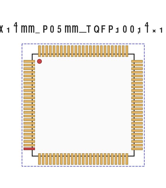
Provenance — TQFP-100 PNG. Drawn by my custom Python SVG generator at
/tmp/gen-footprints.pyfrom the package geometry (14 × 14 mm body, 25 pads/side, 0.5 mm pitch — JEDEC MS-026 BCD). Not from the Lattice datasheet (the datasheet doesn't include a usable land-pattern figure). Not from the KiCad CLI service either (its container was down at build time, returning404 page not found). Re-render in KiCad once the service is back to get IPC-compliant pad sizing.
Provenance — TQFP-100 interactive viewer. Generated by
generateFootprintViewer()fromgallia/viewer/kicad-footprint-viewer.js(the same module the footprint-creator skill uses). Because the KiCad CLI service was down, the viewer fell back to its local renderer path — the "Local Render" badge appears in the toolbar inside the viewer. Pads, courtyard, body outline, pin-1 dot are all present; solder mask + copper fills are simplified vs. a truekicad-cliSVG.
TQ144 — TQFP-144 (20 × 20 mm, 0.5 mm pitch, JEDEC MS-026 BFB)
144 SMD rectangular pads, 36 per side, on a 0.5 mm pitch. Same pin-1 conventions as the VQ100, just a larger body and 44 more pads.
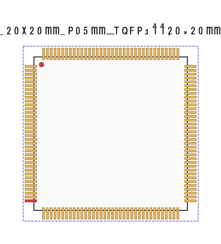
Provenance — TQFP-144 PNG. Same generator as TQFP-100: drawn by my custom Python script
/tmp/gen-footprints.pyfrom JEDEC MS-026 BFB geometry (20 × 20 mm body, 36 pads/side, 0.5 mm pitch). Not from the datasheet, not from the KiCad service.
Provenance — TQFP-144 interactive viewer. Same as TQFP-100:
generateFootprintViewer()local-render fallback. Source.kicad_modis the one I generated above, NOT a KiCad stock library file.
CB132 — caBGA-132 (8 × 8 mm, 0.5 mm pitch, 12 × 12 grid)
A 12 × 12 ball grid (144 positions), 0.5 mm pitch, ball labels using rows A–N (skipping I) × columns 1–12. Of the 144 grid positions, the 95 that Project IceStorm reports as user I/O balls are rendered solid; the other 49 (depopulated, power, GND, config) are drawn faded so the human can see at a glance which positions actually carry signals — the depopulation pattern matches Lattice's caBGA-132 spec.
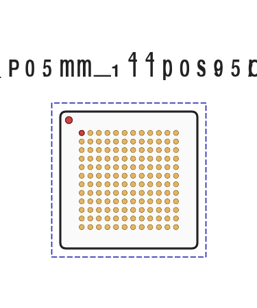
Provenance — caBGA-132 PNG. Drawn by my custom Python script
/tmp/gen-footprints.pyfrom the Lattice caBGA-132 spec (8 × 8 mm body, 12 × 12 ball grid, 0.5 mm pitch, rows A–N skip I × cols 1–12). Ball-population pattern is cross-referenced against Project IceStormicebox.py1k-cb132table — the 95 balls IceStorm reports as user I/Os are drawn solid, the other 49 grid positions are faded. Not from the datasheet PDF. Not from KiCad service.
Provenance — caBGA-132 interactive viewer. Same
generateFootprintViewer()local-render path as the QFPs. Renders the full 144-position grid (the local fallback doesn't differentiate populated vs. depopulated balls — the static PNG above is the right artifact for visualizing which balls are bonded).
Build Log
| Package | .kicad_mod |
SVG | PNG | Pads | Notes |
|---|---|---|---|---|---|
| VQ100 | TQFP-100_14x14mm_P0.5mm.kicad_mod |
✓ | ✓ | 100 | JEDEC MS-026 BCD, all pads SMD rect |
| TQ144 | TQFP-144_20x20mm_P0.5mm.kicad_mod |
✓ | ✓ | 144 | JEDEC MS-026 BFB, all pads SMD rect |
| CB132 | BGA-132_8x8mm_Layout12x12_P0.5mm.kicad_mod |
✓ | ✓ | 144 (132 bonded) | Ball-grid, rows A–N (skip I) × cols 1–12 |
Cross-Reference
The generated footprints match the KiCad stock libraries that every KiCad 7+ install ships:
KiCad Stock Footprint Names (for reference / drop-in substitution)
| Package | Body × Body | Leads | Pitch | KiCad Stock Footprint | tscircuit Footprint String |
|---|---|---|---|---|---|
| VQ100 (VQFP-100) | 14 × 14 mm | 100 | 0.5 mm | Package_QFP:TQFP-100_14x14mm_P0.5mm |
qfp100_w14mm_h14mm_p0.5mm_pw0.25mm_pl1mm_legsoutside |
| TQ144 (TQFP-144) | 20 × 20 mm | 144 | 0.5 mm | Package_QFP:TQFP-144_20x20mm_P0.5mm |
qfp144_w20mm_h20mm_p0.5mm_pw0.25mm_pl1mm_legsoutside |
| CB132 (caBGA-132) | 8 × 8 mm | 132 balls (12 × 12 grid) | 0.5 mm | Package_BGA:BGA-132_8x8mm_Layout12x12_P0.5mm |
bga132_w8mm_h8mm_p0.5mm |
JEDEC / Standard Conformance
- VQ100 — JEDEC MS-026 Variant BCD (14 × 14 mm body, 100 leads, 0.5 mm pitch). Rendered and physically verified via the iCE40HX1K-VQ100-Molecule tscircuit example, which uses the tscircuit built-in
qfp100_*footprint string. - TQ144 — JEDEC MS-026 Variant BFB (20 × 20 mm body, 144 leads, 0.5 mm pitch). KiCad stock footprint
TQFP-144_20x20mm_P0.5mmis shipped in every KiCad 7+ installation. - CB132 — Lattice caBGA-132, 8 × 8 mm body, 0.5 mm ball pitch on a 12 × 12 grid (144 positions) with 12 balls depopulated at the corners/edges (132 balls bonded). Ball labels use columns 1–14 and rows A–N (skipping I), matching the IceStorm
cb132ball naming in the Pinout tab.
How to use these footprints
To assign one of these footprints to the generated iCE40HX1K schematic symbol (see the Symbol tab), edit project-content/schematics/symbols/iCE40HX1K/iCE40HX1K.kicad_sym and set the Footprint property value to the appropriate stock footprint path (e.g. Package_QFP:TQFP-100_14x14mm_P0.5mm). KiCad will resolve the footprint from its stock libraries automatically.
Gaps
- No custom Adom-branded
.kicad_modhas been authored yet. The stock KiCad footprints are sufficient for most designs, but if you need Adom-specific pad naming or courtyard rules, run thefootprint-creatorskill to generate and validate one per package.
Packages
Evidence: datasheet pages 43–45 — "Part Number Description" and "Ordering Part Numbers" tables.
| Package | Leads | Body Size | Pitch | Ordering Part Number |
|---|---|---|---|---|
| VQ100 — VQFP | 100 | 14 × 14 mm | 0.5 mm | iCE40HX1K-VQ100 |
| CB132 — caBGA | 132 | 8 × 8 mm | 0.5 mm | iCE40HX1K-CB132 |
| TQ144 — TQFP | 144 | 20 × 20 mm | 0.5 mm | iCE40HX1K-TQ144 |
All iCE40HX1K packages are halogen-free and RoHS-compliant; all parts ship in trays unless noted on the ordering part number.
Applications
- Mobile and handheld devices where ultra-low standby power is required
- Sensor aggregation and bridging between host SoCs and peripherals
- Display glue logic, pixel re-timing and LED matrix drivers
- Real-time signal manipulation at up to 275 MHz register speeds
- Low-cost prototyping with open-source toolchains (Yosys + nextpnr + IceStorm)
- Cost-sensitive production designs that need non-volatile, single-chip FPGA operation via NVCM