HX711
Unreviewed24-bit delta-sigma ADC for weight scales — dual differential input, PGA gain 32/64/128, 10/80Hz, 2-wire serial, SOP-16
Description
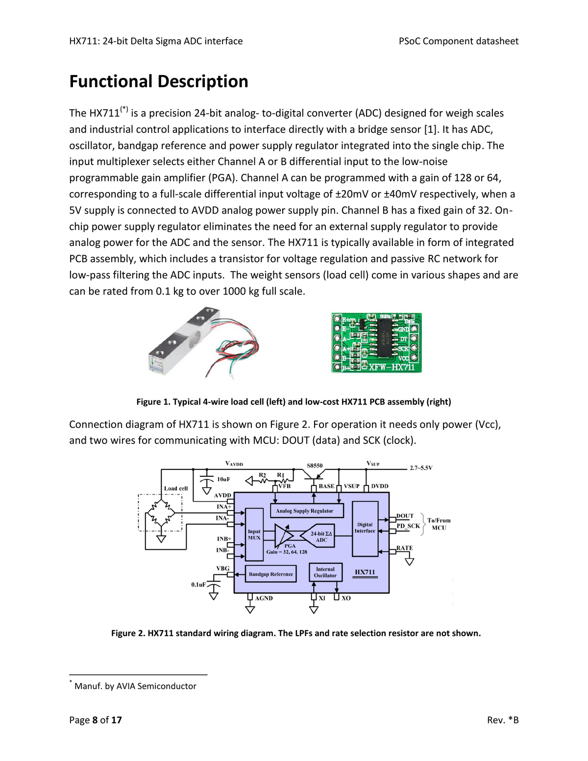
The HX711 is a precision 24-bit analog-to-digital converter (ADC) by AVIA Semiconductor, designed for weigh scales and industrial control applications to interface directly with a bridge sensor. It integrates an ADC, oscillator, bandgap reference, and power supply regulator on a single chip. The input multiplexer selects either Channel A or B differential input to the low-noise programmable gain amplifier (PGA). Channel A supports gains of 128 or 64 (corresponding to full-scale differential input of +/-20 mV or +/-40 mV at 5V AVDD). Channel B has a fixed gain of 32 (+/-80 mV full scale). The on-chip power supply regulator eliminates the need for an external supply regulator for the ADC and sensor.
This datasheet also documents the PSoC Creator software component for interfacing the HX711, providing a ready-to-use driver with interrupt or polling modes.
Features
- 24-bit delta-sigma ADC with two differential input channels
- Selectable gain: 128, 64 (Channel A) or 32 (Channel B)
- Full-scale input: +/-20 mV, +/-40 mV, or +/-80 mV
- On-chip power supply regulator (AVDD from 2.7-5.5V supply)
- Integrated oscillator (no external crystal required)
- Selectable output data rate: 10 Hz or 80 Hz
- Simple 2-wire serial interface (DOUT + PD_SCK)
- Power-down via serial clock input
- Low power: operates from 2.7-5.5V supply
- 16-pin SOP package
Pin Configuration
HX711 IC pinout (SOP-16):
| Pin | Name | Description |
|---|---|---|
| 1 | VSUP | Regulator supply (2.7-5.5V) |
| 2 | BASE | Regulator control |
| 3 | AVDD | Analog supply output |
| 4 | VFB | Regulator feedback |
| 5 | AGND | Analog ground |
| 6 | VBG | Bandgap reference bypass (0.1 uF) |
| 7 | INNA | Channel A negative input |
| 8 | INPA | Channel A positive input |
| 9 | INNB | Channel B negative input |
| 10 | INPB | Channel B positive input |
| 11 | PD_SCK | Serial clock input |
| 12 | DOUT | Serial data output |
| 13 | XO | Crystal oscillator output |
| 14 | XI | Crystal oscillator input |
| 15 | RATE | Output data rate selection (L=10Hz, H=80Hz) |
| 16 | DVDD | Digital supply (2.7-5.5V) |
Electrical Characteristics
ADC Input Channels and Gain
| ADC Gain | Input Channel | Full Scale (mV) |
|---|---|---|
| 128 | A | +/-20 |
| 64 | A | +/-40 |
| 32 | B | +/-80 |
Key Specifications
| Parameter | Value |
|---|---|
| Resolution | 24 bits |
| Output data rate | 10 Hz or 80 Hz |
| Supply voltage | 2.7 - 5.5 V |
| Interface | 2-wire serial (DOUT + PD_SCK) |
| Operating temperature | -40 to +85 C |
Software API
PSoC Creator component API (prefix with instance name, e.g., ADC_1_):
Functions
| Function | Description |
|---|---|
ADC_Start() |
Initialize and start ADC conversion. First 4 readings (400ms at 10 Hz) should be discarded |
ADC_Stop() |
Stop ADC and enter low-current sleep mode |
ADC_GetResult32() |
Read ADC count (raw count minus offset). Call only when data is ready |
ADC_Count_to_mV(value) |
Convert ADC count to millivolts based on selected gain |
ADC_SetOffset(value) |
Set tare offset (subtracted from all readings) |
Variables
| Variable | Description |
|---|---|
ADC_DataReady |
Flag: 1 when data ready for reading (polling mode only). Clears on read |
ADC_Count |
Last ADC reading (raw count minus offset) |
ADC_Gain |
Current PGA gain (128, 64, or 32) |
ADC_Offset |
Current tare offset value |
Communication Protocol
The 2-wire interface uses DOUT (data) and PD_SCK (clock):
- 24 clock pulses read 24 bits of data (MSB first)
- 1-3 additional clocks set the gain for the next conversion (25 clocks = gain 128, 26 = gain 32, 27 = gain 64)
- Single conversion takes approximately 600 CPU clocks (13 us at 48 MHz)
Applications
- Weight scales and load cell measurement
- Industrial control and process measurement
- Bio-potential and ECG signal acquisition
- Any application requiring high-precision measurement of small DC signals