CD74HC4067 — 16-Channel Analog Multiplexer / Demultiplexer
UnreviewedTI CD74HC4067. 16-channel bidirectional analog mux/demux, 70 Ω typ R(on), break-before-make, 2–6 V HC or 4.5–5.5 V HCT. 24-pin PDIP/SOIC/SSOP/TSSOP.
Source: Texas Instruments CD74HC4067 / CD74HCT4067 Datasheet
Manufacturer: Texas Instruments
Part Number: CD74HC4067 (HCT variant: CD74HCT4067)
Document: SCHS209D — November 1998, Revised December 2024 (High-Speed CMOS Logic 16-Channel Analog Multiplexer and Demultiplexer)
Description
The CD74HC4067 and CD74HCT4067 devices are digitally controlled analog switches that use silicon-gate CMOS technology to achieve operating speeds similar to LSTTL, with the low power consumption of standard CMOS integrated circuits.
These analog multiplexers and demultiplexers control analog voltages that may vary across the voltage supply range. They are bidirectional switches, thus allowing any analog input to be used as an output and vice versa. The switches have low on-resistance and low off leakages. In addition, these devices have an enable control that, when high, disables all switches to their off state.
Key Specifications
| Parameter | Value |
|---|---|
| Channels | 16 (analog mux/demux, bidirectional) |
| Supply Voltage (HC) | 2 V to 6 V (analog input up to VCC) |
| Supply Voltage (HCT) | 4.5 V to 5.5 V |
| On-Resistance (typ) | 70 Ω @ VCC = 4.5 V; 60 Ω @ VCC = 6 V |
| CMOS input compatibility | II ≤ 1 µA at VOL, VOH |
| LSTTL input drive loads | 15 |
| Direct LSTTL input logic compatibility | VIL ≤ 0.8 V (max), VIH ≥ 2 V (min) @ VCC = 4.5 V to 5.5 V |
| High noise immunity | NIL = 30 %, NIH = 30 % of VCC @ VCC = 5 V |
| Fanout (over-temperature range) | 10 LSTTL standard outputs; 15 LSTTL bus-driver outputs |
| Wide operating temperature range | −55 °C to +125 °C |
| Propagation delay / switching time | ~6 ns (typ) at 4.5 V, balanced |
| Packages | PDIP (E), SOIC (M), SSOP (SM), TSSOP (PW) — 24-pin |
Features
- Wide analog input voltage range
- Low ON resistance: VCC = 4.5 V → 70 Ω (typ); VCC = 6 V → 60 Ω (typ)
- Fast switching propagation speeds
- Break-before-make switching (6 ns typ at 4.5 V)
- Available in both narrow- and wide-body plastic packages
- Fanout (over-temperature range): 10 LSTTL (std) / 15 LSTTL (bus-drive)
- Wide operating temperature range: −55 °C to 125 °C
- Balanced propagation delay and transition times
- Significant power reduction compared to LSTTL logic ICs
- HC types: 2 V to 6 V operation; high noise immunity 30 % of VCC
- HCT types: 4.5 V to 5.5 V operation; direct LSTTL-input logic compatibility and CMOS input compatibility
Applications
- Signal gating
- Modulators
- Squelch controls
- Demodulators
- Choppers
- Commutating switches
- Analog-to-digital and digital-to-analog conversions
- Digital control of frequency, impedance, phase, and analog-signal gain
- Energy infrastructure
- Building automation
- Wireless infrastructure
- Appliances
- Data center & enterprise computing
- Retail automation & payment
Pin Configuration
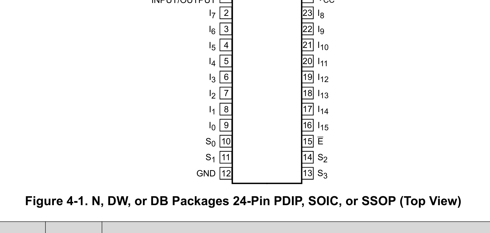
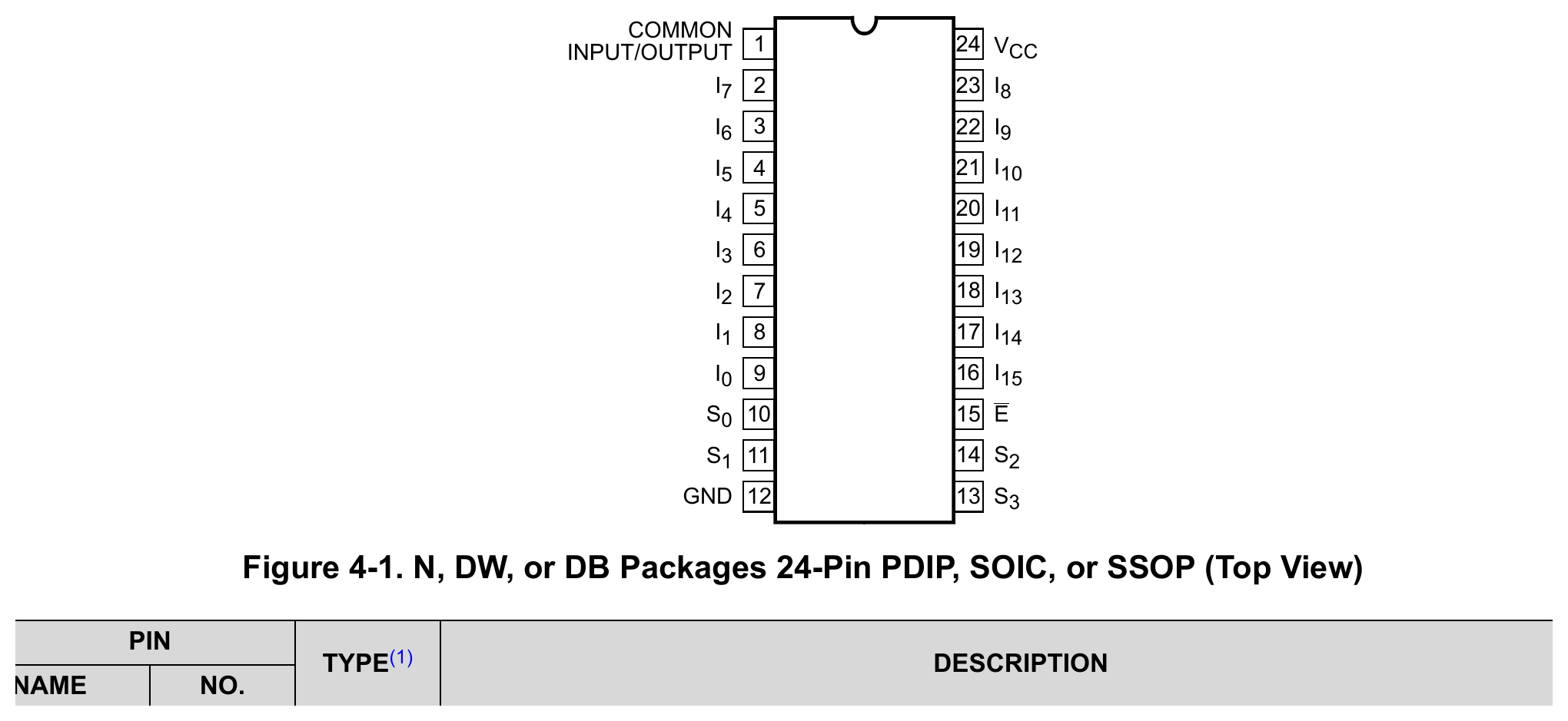
24-pin PDIP (N, DW, DB), SOIC, or SSOP top view.
| Pin | Name | Type | Description |
|---|---|---|---|
| 1 | COMMON INPUT/OUTPUT | IO | Common input or output |
| 2 | I7 | IO | Switch input/output |
| 3 | I6 | IO | Switch input/output |
| 4 | I5 | IO | Switch input/output |
| 5 | I4 | IO | Switch input/output |
| 6 | I3 | IO | Switch input/output |
| 7 | I2 | IO | Switch input/output |
| 8 | I1 | IO | Switch input/output |
| 9 | I0 | IO | Switch input/output |
| 10 | S0 | I | Select / Address pin |
| 11 | S1 | I | Select / Address pin |
| 12 | GND | P | Ground pin |
| 13 | S2 | I | Select / Address pin |
| 14 | S3 | I | Select / Address pin |
| 15 | E | I | Enable for all switches ON/OFF (active low) |
| 16 | I15 | IO | Switch input/output |
| 17 | I14 | IO | Switch input/output |
| 18 | I13 | IO | Switch input/output |
| 19 | I12 | IO | Switch input/output |
| 20 | I11 | IO | Switch input/output |
| 21 | I10 | IO | Switch input/output |
| 22 | I9 | IO | Switch input/output |
| 23 | I8 | IO | Switch input/output |
| 24 | VCC | P | Power pin |
Thermal Information
| Thermal Metric | E (PDIP, 24 pins) | M (SOIC, 24 pins) | SM (SSOP, 24 pins) | PW (TSSOP, 24 pins) | Unit |
|---|---|---|---|---|---|
| RθJA | 67 | 84.8 | 96.2 | 97.4 | °C/W |
| RθJC(top) | N/A | 57.0 | 60.0 | 45.0 | °C/W |
| RθJB | N/A | 59.5 | 65.1 | 62.7 | °C/W |
| ΨJT | N/A | 29.0 | 21.1 | 5.20 | °C/W |
| ΨJB | N/A | 59.0 | 64.4 | 62.1 | °C/W |
Recommended Operating Conditions
| Parameter | Symbol | Conditions | Min | Nom | Max | Unit |
|---|---|---|---|---|---|---|
| Supply Voltage Range | VCC | CD54 and 74HC types | 2 | — | 6 | V |
| Supply Voltage Range | VCC | CD54 and 74HCT types | 4.5 | — | 5.5 | V |
| Analog Switch I/O Voltage | VIS | 0 | — | VCC | V | |
| Ambient Temperature | TA | −55 | — | 125 | °C | |
| Input Rise and Fall Times | tr, tf | 2 V | 0 | — | 1000 | ns |
| Input Rise and Fall Times | tr, tf | 4.5 V | 0 | — | 500 | ns |
| Input Rise and Fall Times | tr, tf | 6 V | 0 | — | 400 | ns |
Package Information
| Part Number | Package | Body Size (NOM) |
|---|---|---|
| CD74HC4067M | SOIC (24) | 15.4 mm × 10.3 mm |
| CD74HC4067M96 | SOIC (24) | 15.4 mm × 10.3 mm |
| CD74HC4067PW | TSSOP (24) | 7.8 mm × 6.4 mm |
| CD74HCT4067M | SOIC (24) | 15.4 mm × 10.3 mm |
| CD74HCT4067M96 | SOIC (24) | 8.20 mm × 7.40 mm |
| CD74HCT4067PW | TSSOP (24) | 7.8 mm × 6.4 mm |