BQ76952 Battery Monitor and Protector
UnreviewedTexas Instruments BQ76952 battery monitor/protector for 3s-16s Li-ion, Li-polymer, and LiFePO4 packs. Exhaustive extraction with full pin table, expanded design guidance, and all 26 figure-bearing dat
Symbol & Footprint
Schematic
BQ76952 — Parsed Datasheet
Source: Texas Instruments BQ76952 Datasheet (SLUSE13B)
Manufacturer: Texas Instruments
Document: SLUSE13B — Revised November 2021
Part Number: BQ76952
Package: PFB (48-pin TQFP), 7 mm × 7 mm
Description
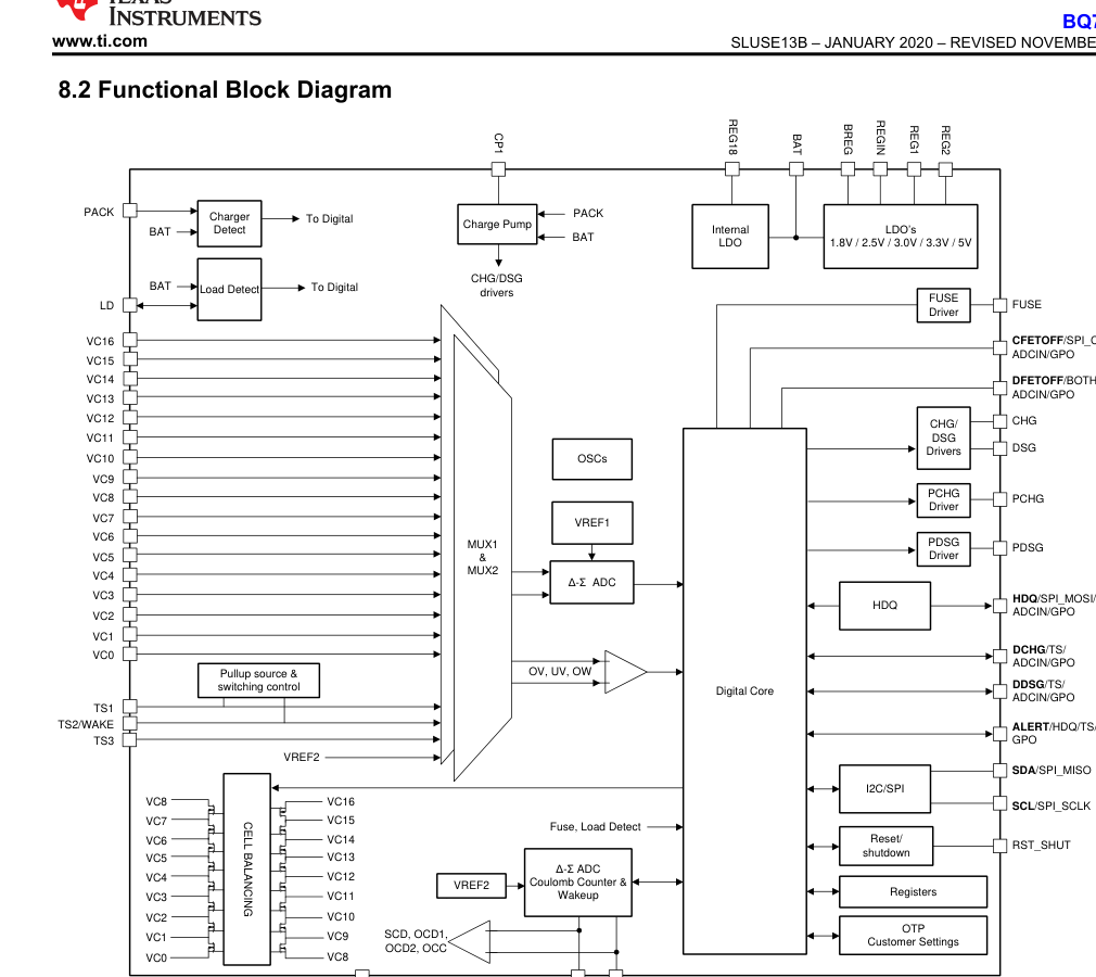
The BQ76952 is a highly integrated battery monitor and protection IC for 3-series to 16-series Li-ion, Li-polymer, and LiFePO4 battery packs. It combines high-accuracy cell and pack measurements, coulomb counting, configurable protection logic, autonomous or host-controlled cell balancing, and high-side FET gate-drive support in a 48-pin TQFP package.
Alongside measurement and protection functions, the device integrates a charge pump for CHG and DSG NFET control, precharge and predischarge drivers, a secondary fuse driver, dual programmable LDOs for external circuitry, and host communications over I2C, SPI, or HDQ. The BQ76952 family also includes factory-configured variants that change the default communications mode and REG1 startup behavior.
Device Comparison Table
| Part Number | Default Interface | CRC Enabled | REG1 Default |
|---|---|---|---|
| BQ76952 | I2C | No | Disabled |
| BQ7695201 | SPI | Yes | Disabled |
| BQ7695202 | I2C | Yes | Enabled, 3.3 V |
| BQ7695203 | SPI | Yes | Enabled, 5 V |
| BQ7695204 | SPI | Yes | Enabled, 3.3 V |
Key Specifications
| Parameter | Value |
|---|---|
| Supported battery stack | 3 to 16 series Li-ion, Li-polymer, or LiFePO4 cells |
| BAT supply voltage | 4.7 V to 80 V |
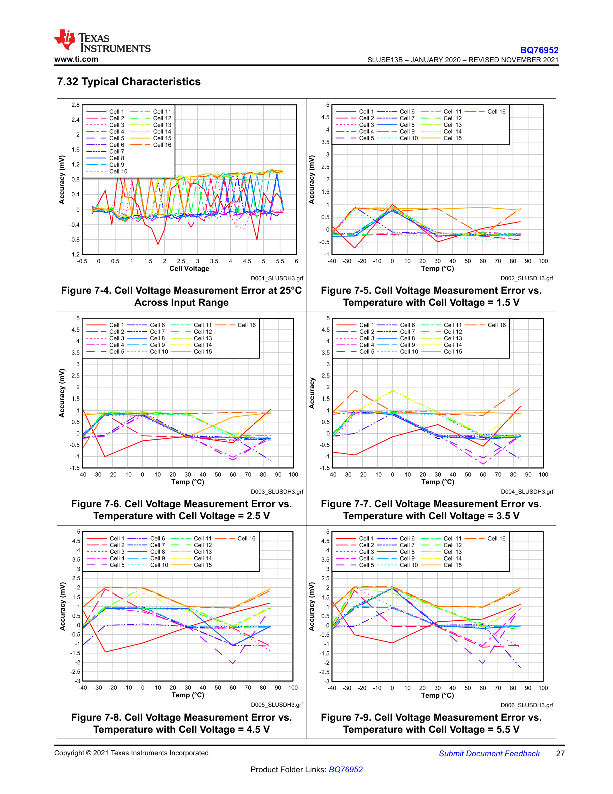
| Cell voltage accuracy | ±5 mV typ at 25°C; ±10 mV max from 0°C to 60°C; ±15 mV max from -40°C to 85°C |
| Current-sense range | ±200 mV across the shunt resistor |
| Coulomb counter offset | < 1 µV typ (feature summary) |
| Communications | I2C up to 400 kHz, SPI, HDQ one-wire |
| Programmable LDOs | REG1 and REG2 selectable to 1.8 V, 2.5 V, 3.0 V, 3.3 V, or 5.0 V |
| Low-power modes | 286 µA normal, 24 µA to 41 µA sleep, 9.2 µA to 10.7 µA deep sleep, 1 µA typ shutdown |
| Temperature sensing | Internal temperature sensor plus support for up to nine external thermistors |
| Package | PFB 48-pin TQFP, 7 mm × 7 mm |
Features
- Battery monitoring capability for 3-series to 16-series cells
- Extensive protection coverage for voltage, temperature, current, fuse, and internal diagnostics
- Two independent ADC paths for synchronized voltage and current sampling
- Autonomous or host-controlled cell balancing
- Integrated charge pump for high-side NFET protection control
- Integrated precharge, predischarge, and secondary chemical fuse drive support
- High-voltage tolerance up to 85 V on battery-stack related pins
- Random cell attach sequence tolerance for production environments
- Customer-programmable OTP memory for manufacturing-time configuration
- Dual programmable LDOs for external host and support circuitry
Pin Configuration
| Pin | Name | Type | Description |
|---|---|---|---|
| 1 | VC15 | Input | Sense input for cell 15; also balancing path for cell 15 and return path for cell 16 |
| 2 | VC14 | Input | Sense input for cell 14; also balancing path for cell 14 and return path for cell 15 |
| 3 | VC13 | Input | Sense input for cell 13; also balancing path for cell 13 and return path for cell 14 |
| 4 | VC12 | Input | Sense input for cell 12; also balancing path for cell 12 and return path for cell 13 |
| 5 | VC11 | Input | Sense input for cell 11; also balancing path for cell 11 and return path for cell 12 |
| 6 | VC10 | Input | Sense input for cell 10; also balancing path for cell 10 and return path for cell 11 |
| 7 | VC9 | Input | Sense input for cell 9; also balancing path for cell 9 and return path for cell 10 |
| 8 | VC8 | Input | Sense input for cell 8; also balancing path for cell 8 and return path for cell 9 |
| 9 | VC7 | Input | Sense input for cell 7; also balancing path for cell 7 and return path for cell 8 |
| 10 | VC6 | Input | Sense input for cell 6; also balancing path for cell 6 and return path for cell 7 |
| 11 | VC5 | Input | Sense input for cell 5; also balancing path for cell 5 and return path for cell 6 |
| 12 | VC4 | Input | Sense input for cell 4; also balancing path for cell 4 and return path for cell 5 |
| 13 | VC3 | Input | Sense input for cell 3; also balancing path for cell 3 and return path for cell 4 |
| 14 | VC2 | Input | Sense input for cell 2; also balancing path for cell 2 and return path for cell 3 |
| 15 | VC1 | Input | Sense input for cell 1; also balancing path for cell 1 and return path for cell 2 |
| 16 | VC0 | Input | Sense input for the negative terminal of cell 1; return path for cell-1 balancing current |
| 17 | VSS | Power | Device ground |
| 18 | SRP | Input | Top-side current-sense input for coulomb counting and current protections |
| 19 | NC | None | Not connected internally |
| 20 | SRN | Input | Bottom-side current-sense input for coulomb counting and current protections |
| 21 | TS1 | I/O | Thermistor input or general-purpose ADC input |
| 22 | TS2 | I/O | Thermistor input, shutdown wake input, or general-purpose ADC input |
| 23 | TS3 | I/O | Thermistor input or general-purpose ADC input |
| 24 | REG18 | Power | Internal 1.8 V LDO output/reference rail |
| 25 | ALERT | I/O | ALERT output, HDQ I/O, thermistor/ADC input, or digital output depending on configuration |
| 26 | SCL | I/O | I2C SCL or SPI SCLK |
| 27 | SDA | I/O | I2C SDA or SPI MISO |
| 28 | HDQ | I/O | HDQ I/O, SPI MOSI, thermistor/ADC input, or digital output |
| 29 | CFETOFF | I/O | Charge-FET-off input, SPI CS, thermistor/ADC input, or digital output |
| 30 | DFETOFF | I/O | Discharge-FET-off/BOTHOFF input, thermistor/ADC input, or digital output |
| 31 | DCHG | I/O | Digital charge-status output, thermistor/ADC input, or digital output |
| 32 | DDSG | I/O | Digital discharge-status output, thermistor/ADC input, or digital output |
| 33 | RST_SHUT | Input | Reset and shutdown control input |
| 34 | REG2 | Power | Programmable LDO output; selectable to 1.8 V, 2.5 V, 3.0 V, 3.3 V, or 5.0 V |
| 35 | REG1 | Power | Programmable LDO output; selectable to 1.8 V, 2.5 V, 3.0 V, 3.3 V, or 5.0 V |
| 36 | REGIN | Input | Input rail feeding REG1 and REG2 |
| 37 | BREG | Output | Base-drive/control output for the external preregulator transistor |
| 38 | FUSE | I/O | Fuse sense and fuse-drive pin |
| 39 | PDSG | Output | Predischarge PFET control output |
| 40 | PCHG | Output | Precharge PFET control output |
| 41 | LD | I/O | Load-detect input and wake-related multifunction pin |
| 42 | PACK | Input | Pack-voltage sense input |
| 43 | DSG | Output | Main NMOS discharge-FET drive |
| 44 | NC | None | Not connected internally |
| 45 | CHG | Output | Main NMOS charge-FET drive |
| 46 | CP1 | I/O | Charge-pump capacitor connection |
| 47 | BAT | Power | Primary device supply input |
| 48 | VC16 | Input | Sense input for cell 16, balancing path for cell 16, and top-of-stack measurement point |
Absolute Maximum Ratings
| Parameter | Min | Max | Unit |
|---|---|---|---|
| BAT supply voltage | VSS - 0.3 | VSS + 85 | V |
| PACK, LD input voltage | VSS - 0.3 | VSS + 85 | V |
| PCHG, PDSG input voltage | max(VBAT - 10, VLD - 10) | VSS + 85 | V |
| FUSE input voltage | VSS - 0.3 | min(VSS + 20, VBAT + 0.3) | V |
| REG1, REG2, RST_SHUT, ALERT, SCL, SDA, HDQ, CFETOFF, DFETOFF, DCHG, DDSG | VSS - 0.3 | VSS + 6 | V |
| SRP, SRN | VSS - 0.3 | VREG18 + 0.3 | V |
Recommended Operating Conditions
| Parameter | Min | Typ | Max | Unit |
|---|---|---|---|---|
| BAT supply voltage | 4.7 | — | 80 | V |
| OTP programming supply voltage | 10 | — | 12 | V |
| PACK, LD input range | 0 | — | 80 | V |
| Current-sense differential range (SRP - SRN) | -0.2 | — | 0.2 | V |
| External cell input resistance | 20 | — | 100 | Ω |
| External cell input capacitance | 0.1 | 0.22 | 1 | µF |
| Operating temperature | -40 | — | 85 | °C |
Electrical Characteristics
| Parameter | Conditions | Min | Typ | Max | Unit |
|---|---|---|---|---|---|
| Cell voltage measurement accuracy | 2 V < VCELL < 5 V, TA = 25°C | -5 | — | 5 | mV |
| Cell voltage measurement accuracy | 2 V < VCELL < 5 V, TA = 0°C to 60°C | -10 | — | 10 | mV |
| Cell voltage measurement accuracy | -0.2 V < VCELL < 5.5 V, TA = -40°C to 85°C | -15 | — | 15 | mV |
| Stack voltage measurement accuracy | 0 V < VC16 - VSS < 80 V | -0.5 | — | 0.5 | V |
| PACK pin voltage measurement accuracy | 0 V < VPACK < 80 V | -0.5 | — | 0.5 | V |
| LD pin voltage measurement accuracy | 0 V < VLD < 80 V | -0.5 | — | 0.5 | V |
| Coulomb counter input range | VSRP - VSRN | -0.2 | — | 0.2 | V |
| Coulomb counter effective input resistance | — | — | 2 | — | MΩ |
| Current-wake threshold error | Threshold setting between ±0.5 mV and ±5 mV | -200 | — | 200 | µV |
| ADC input range, cell differential mode | Internal VREF1 | -0.2 | — | 5.5 | V |
Power Consumption
| Mode | Conditions | Typ | Max | Unit |
|---|---|---|---|---|
| Normal | Regular measurements and protections active | 286 | — | µA |
| Sleep 1 | Periodic protections and monitoring, DSG on in 11 V overdrive mode | 41 | — | µA |
| Sleep 2 | Periodic protections and monitoring, DSG in source-follower mode | 24 | — | µA |
| Deep sleep 1 | No monitoring or protections, LFO on | 10.7 | — | µA |
| Deep sleep 2 | No monitoring or protections, LFO off | 9.2 | — | µA |
| Shutdown | TS2 wake circuit active, no monitoring or communications | 1 | 3.1 | µA |
Power Domains
| Rail / Block | Configuration | Range / Nominal | Notes |
|---|---|---|---|
| REG18 | Internal LDO | 1.6 V to 2.0 V, 1.8 V typ | Reference rail for low-voltage functions and thermistor/ADC domains |
| REG1 | Programmable LDO | 1.8 V, 2.5 V, 3.0 V, 3.3 V, or 5.0 V nominal; up to 45 mA load | Can power an external MCU or support circuitry |
| REG2 | Programmable LDO | 1.8 V, 2.5 V, 3.0 V, 3.3 V, or 5.0 V nominal; up to 45 mA load | Independent second LDO for auxiliary rails |
| REG0 / BREG / REGIN path | Preregulator | Internal BREG-controlled preregulator or external 5.5 V REGIN supply | Feeds REG1 and REG2 |
| Charge pump / CP1 | Gate-drive boost | Supports CHG and DSG high-side NFET drive | Startup and load behavior depend on CP1 capacitance |
Thermal Information
| Package | RθJA | RθJC(top) | RθJB | ΨJT | ΨJB | Unit |
|---|---|---|---|---|---|---|
| PFB (48-pin TQFP) | 66.0 | 19.6 | 29.3 | 0.8 | 29.1 | °C/W |
Communication Interface
| Interface | Notes | Pin Mapping |
|---|---|---|
| I2C | Supports 100 kHz and 400 kHz operation; base BQ76952 defaults to I2C without CRC | SDA, SCL |
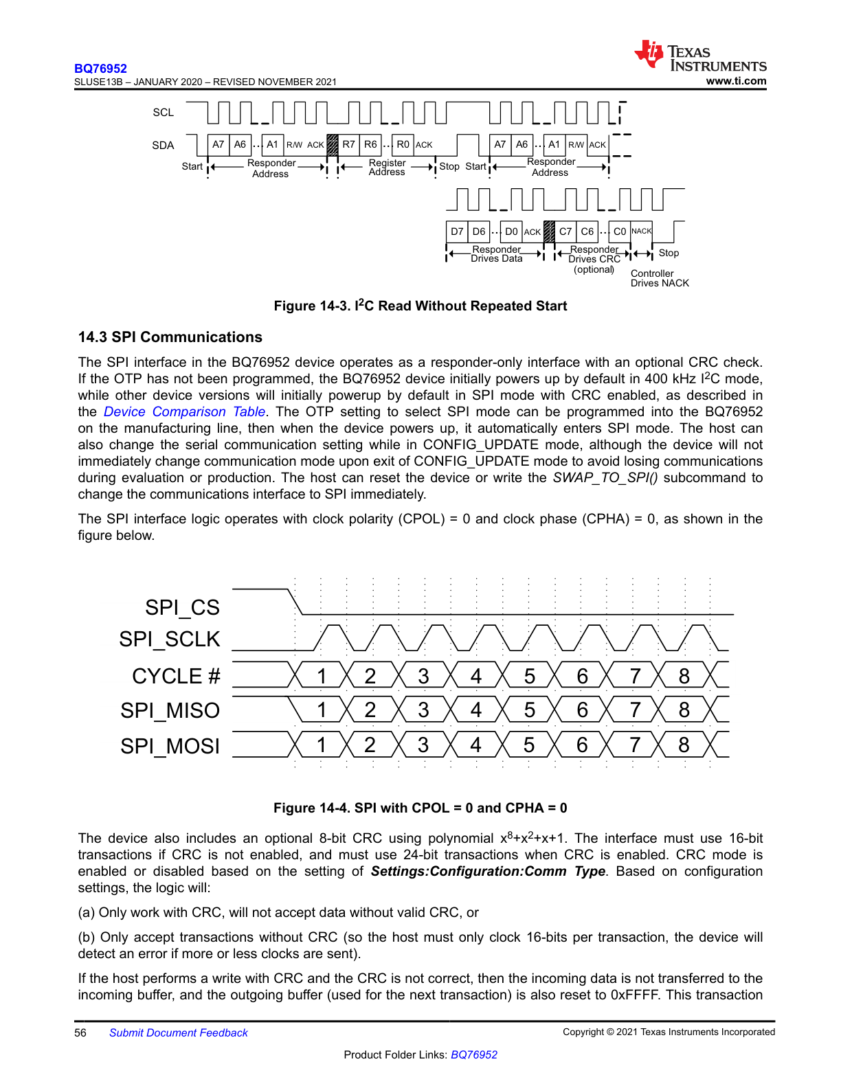
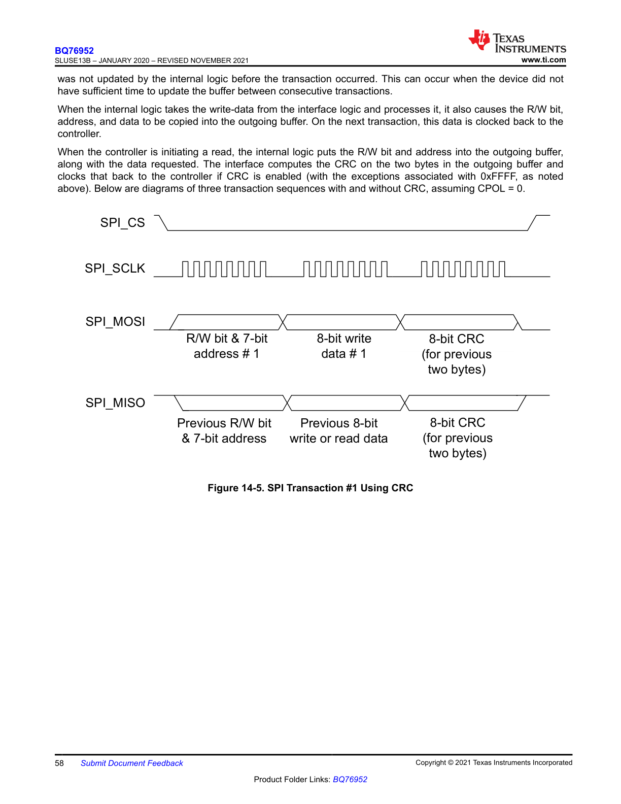
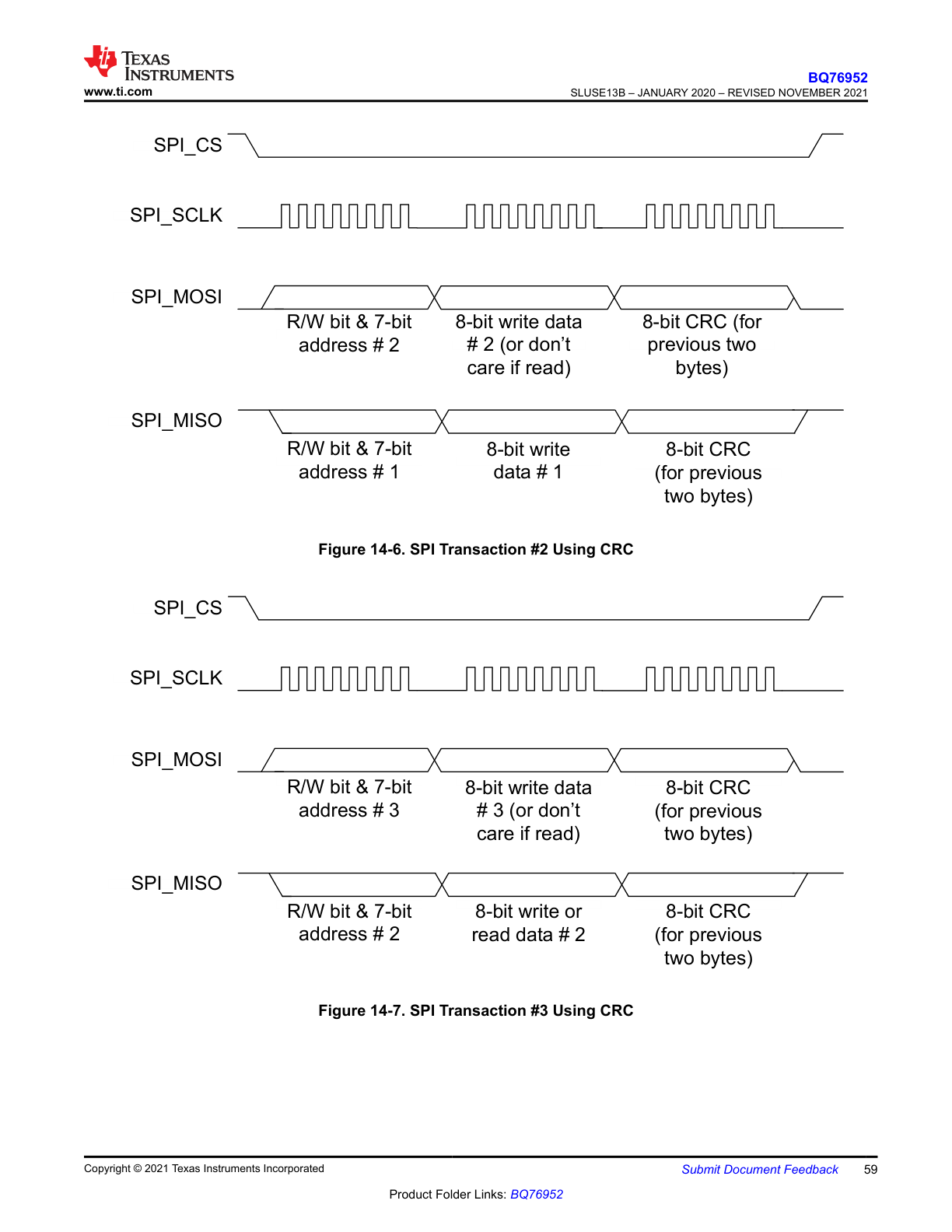
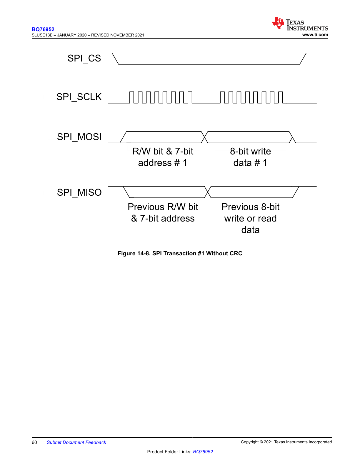
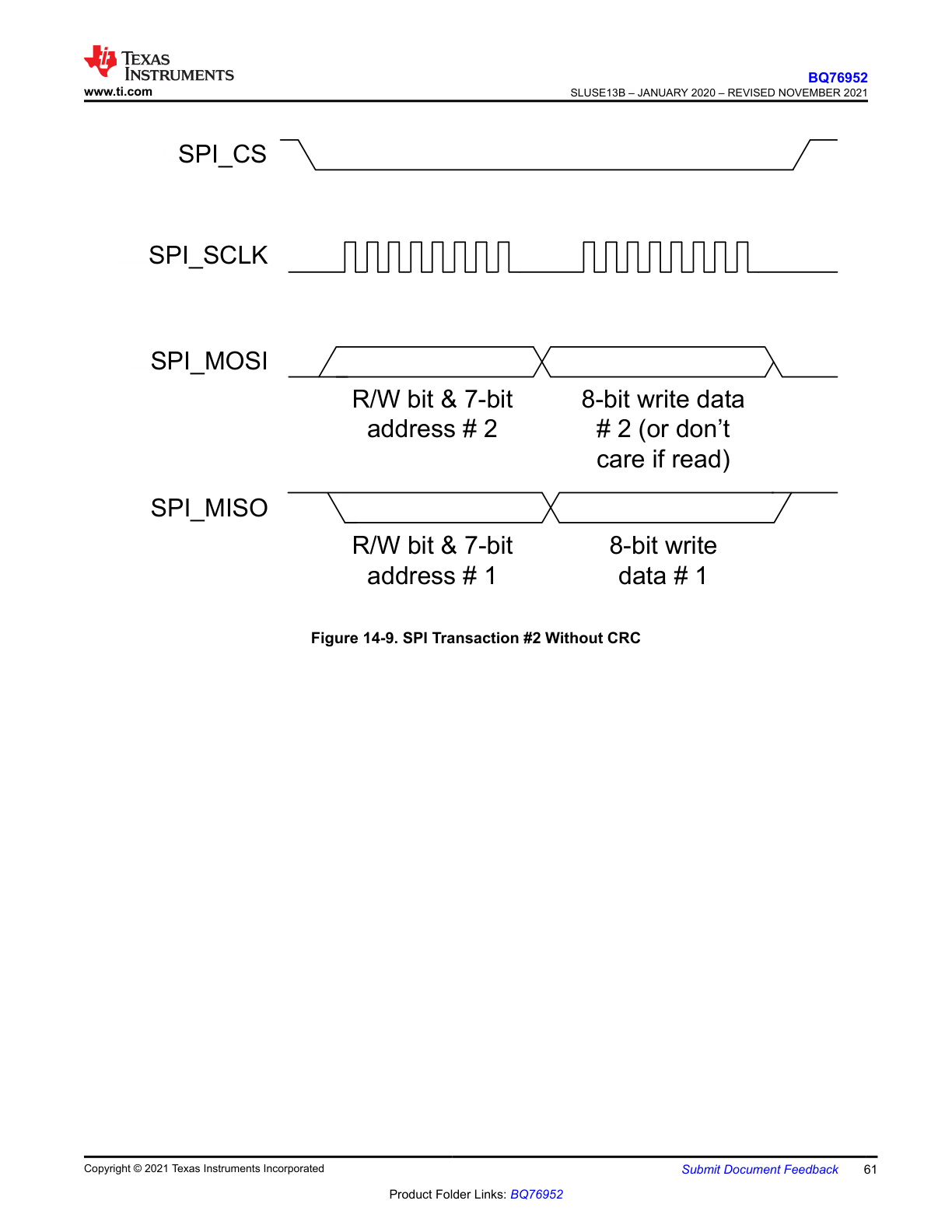
| SPI | Responder-only interface with optional CRC; uses CPOL = 0 and CPHA = 0 | SDA = MISO, SCL = SCLK, HDQ = MOSI, CFETOFF = CS |
| HDQ | Single-wire asynchronous responder interface with open-drain signaling | HDQ or ALERT, depending on configuration |
Serial Transaction Coverage
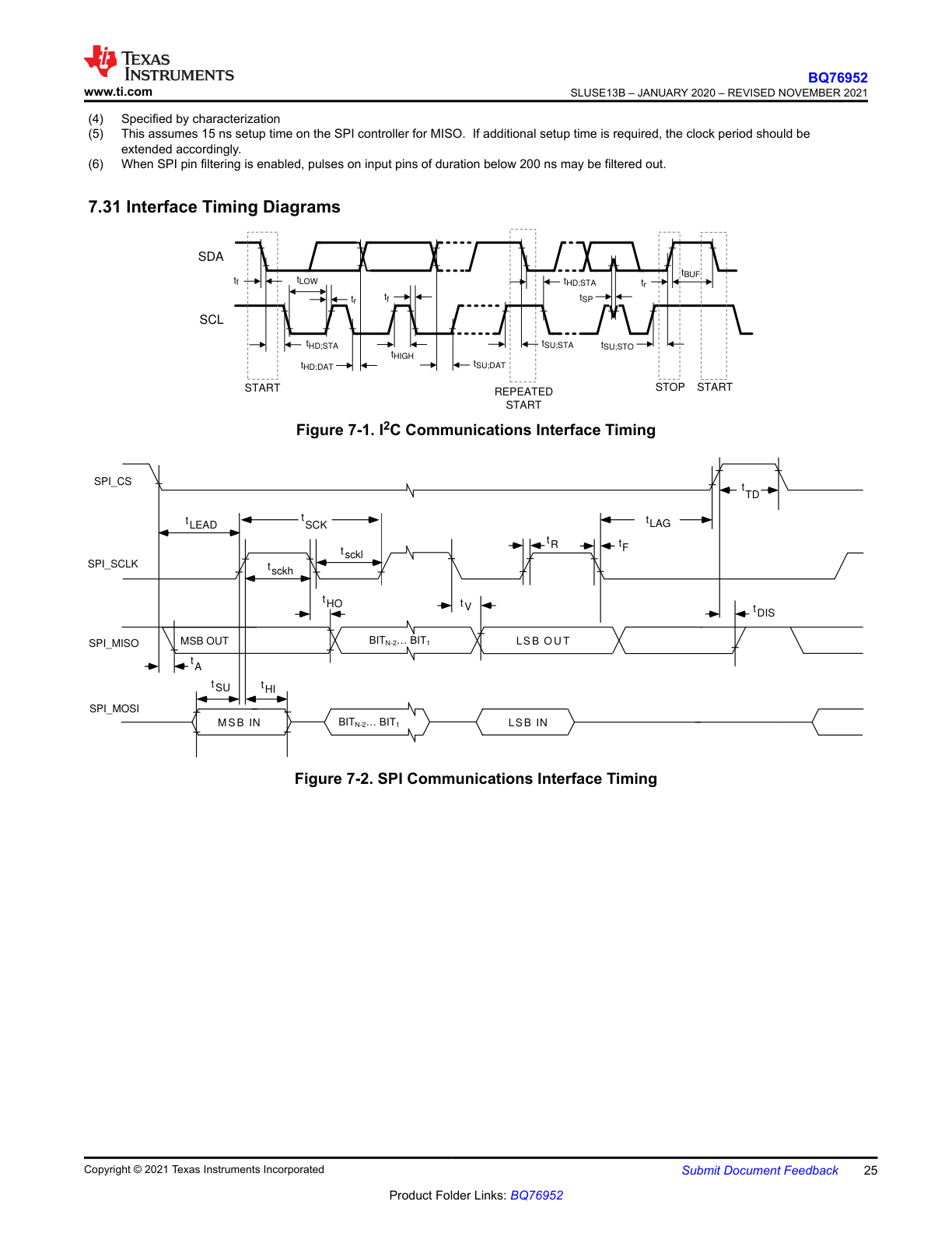
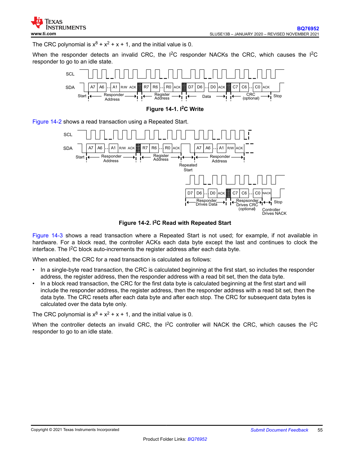
- I2C timing requirements are provided for 100 kHz and 400 kHz operation, including repeated-start and non-repeated-start read sequences.
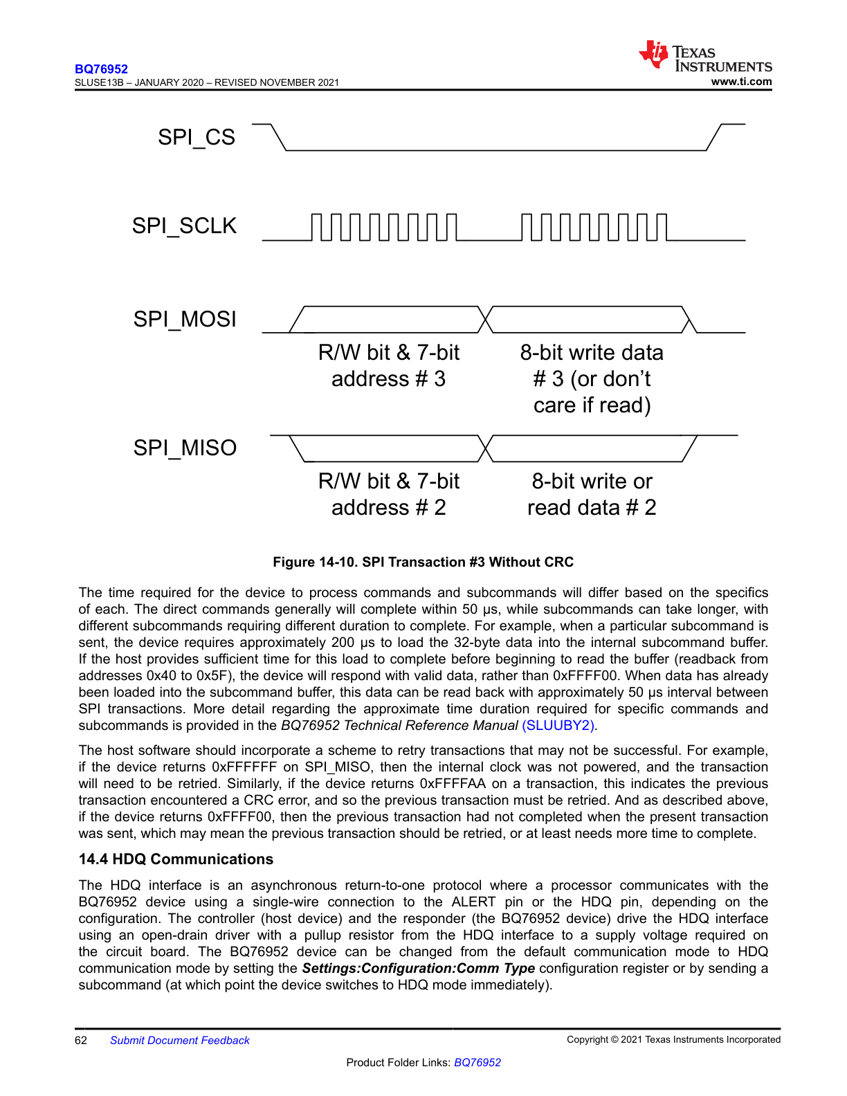
- SPI timing is documented with and without CRC, including responder timing, bus-reset behavior, and MISO drive considerations.
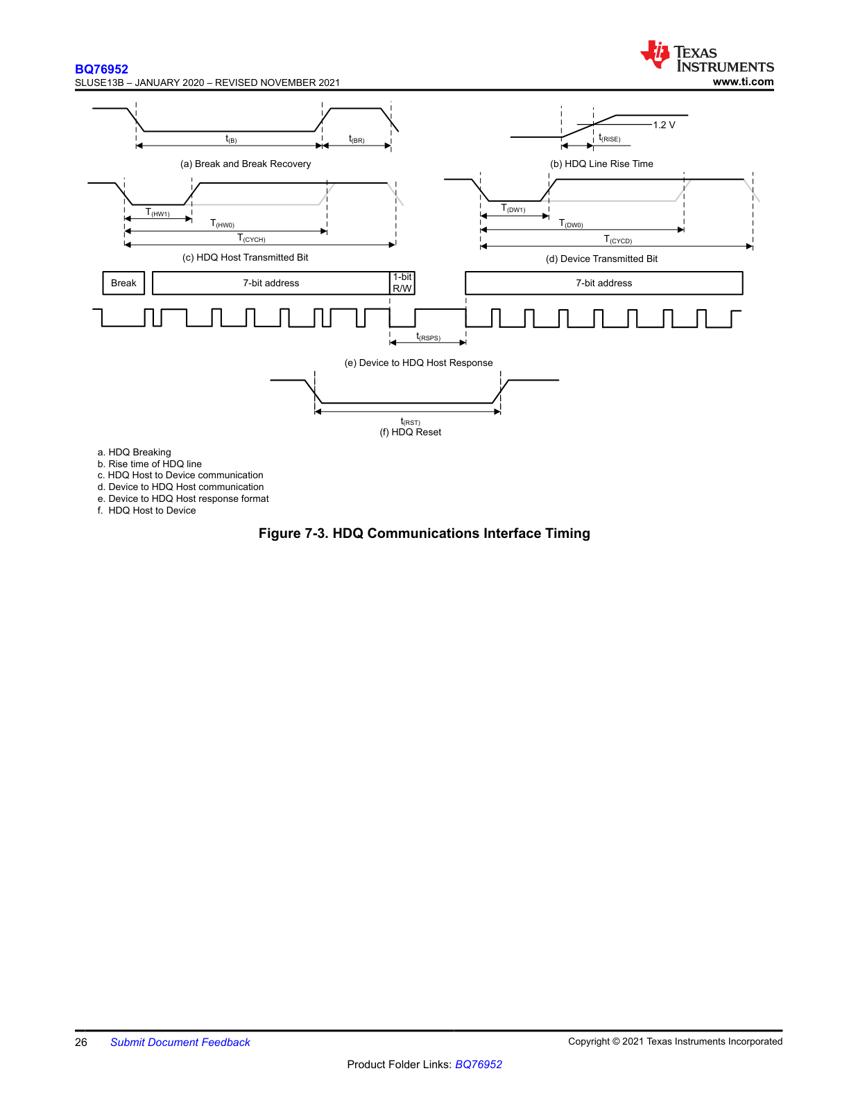
- HDQ is documented as a responder-only single-wire protocol with explicit break, command, and response timing.
Measurement Subsystem
| Function | Summary |
|---|---|
| Cell voltage ADC | Measures up to 16 differential cell voltages in a 3s to 16s stack; recommended input range is -0.2 V to 5.5 V per cell channel |
| Measurement loop | Scans all 16 cells, then auxiliary nodes such as VC16, PACK, LD, internal references, and enabled thermistor / ADCIN inputs |
| Loop timing | Each voltage slot takes about 3 ms, or 1.5 ms with fast ADC enabled; a full loop is typically 18 to 21 slots |
| Current measurement | Dedicated coulomb-counter ADC measures shunt voltage continuously over a ±200 mV range |
| CC1 / CC2 / CC3 filters | CC1 provides lower-rate integrated-current data, CC2 provides fast current data, and CC3 averages a programmable number of CC2 samples |
| Synchronized measurements | Current samples can be paired with cell voltage measurements for impedance analysis and diagnostics |
| ADCIN inputs | TS1, TS2, TS3, ALERT, HDQ, CFETOFF, DFETOFF, DCHG, and DDSG can be repurposed as auxiliary ADC inputs when not used for digital functions |
Protection Architecture
| Protection group | Coverage |
|---|---|
| Primary protections | Cell undervoltage / overvoltage, overcurrent in charge, multiple overcurrent-in-discharge tiers, short circuit in discharge, charge/discharge temperature protections, internal and FET overtemperature, watchdog, and precharge timeout |
| Secondary protections | Permanent-fail checks for safety cell voltage, safety current, safety temperature, imbalance, OTP / ROM / reference / oscillator faults, commanded PF, and other critical diagnostics |
| FET control | Supports autonomous, partially autonomous, or host-managed CHG / DSG FET control |
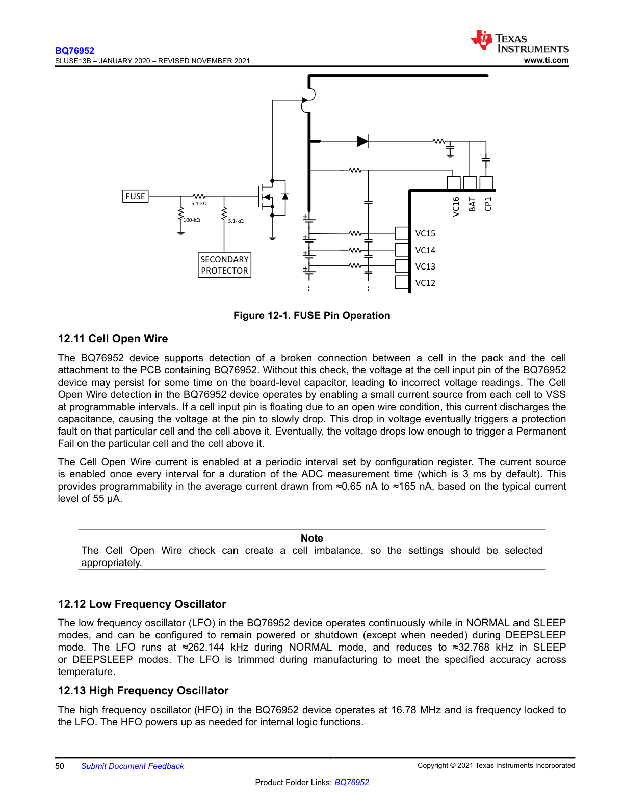
| Fuse behavior | Permanent fail can flag only, latch off FETs, or assert the FUSE output to permanently disable the pack |
| Driver topology | Integrated charge pump drives high-side NFET charge and discharge FETs; also supports precharge and predischarge PFET control |
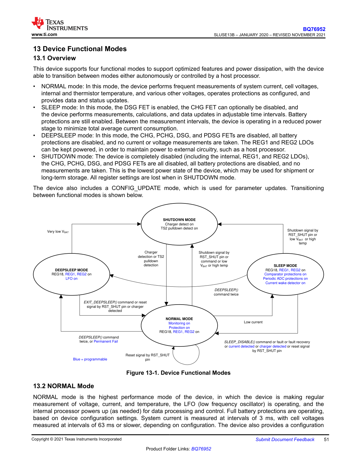
Device Functional Modes
| Mode | Behavior |
|---|---|
| NORMAL | Full measurements, protections, communications, and active pack-management behavior |
| SLEEP | Reduced-power monitoring with periodic measurements and configurable wake behavior |
| DEEPSLEEP | Lower-power standby with monitoring/protection largely disabled, preserving configuration/state as applicable |
| SHUTDOWN | Minimum-current mode with TS2 / LD based wake mechanisms and communications off |
| CONFIG_UPDATE | Register/configuration update mode used during setup and manufacturing configuration |
Cell Balancing
- Supports passive cell balancing using integrated bypass switches or external bypass FETs.
- Can operate in autonomous voltage-based balancing mode or under explicit host control.
- Autonomous balancing is limited to non-adjacent active cells; host-controlled balancing can drive adjacent cells.
- Balancing is temporarily paused around affected ADC measurements to protect voltage accuracy.
- Configuration can limit the maximum number of simultaneously balanced cells to control device heating.
Typical Implementation
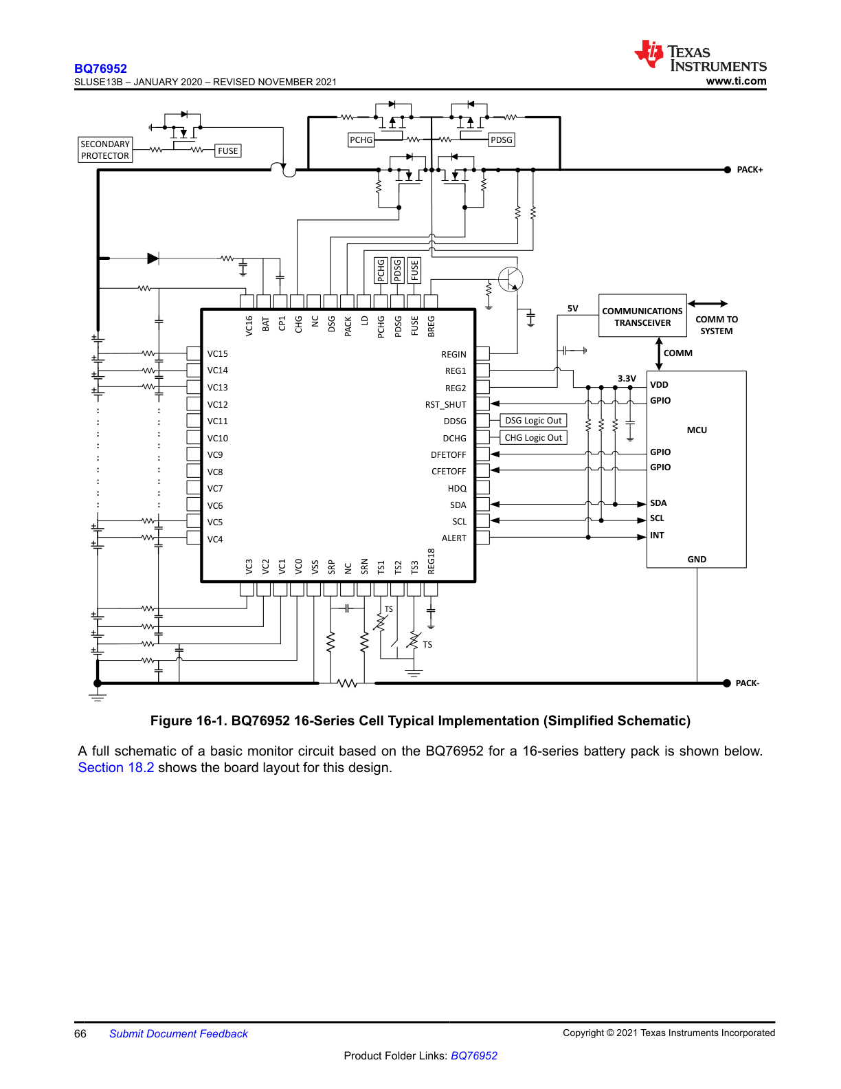
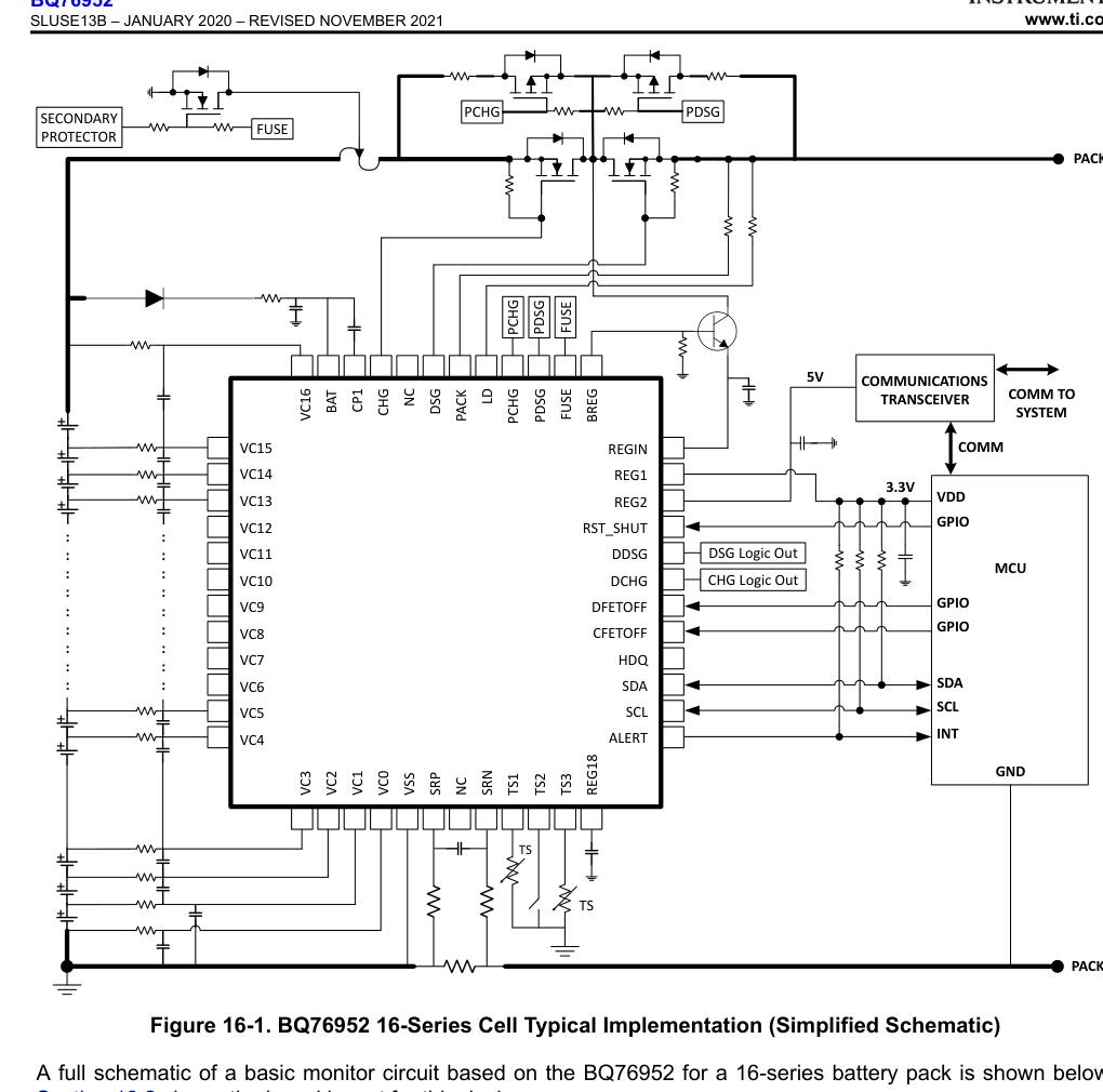
The reference application in the datasheet shows the BQ76952 in a 16-series battery pack with an external secondary protector, host MCU, and communications transceiver. The example design uses CHG and DSG high-side FETs in series, plus dedicated precharge and predischarge PFET paths, and routes the REG1 / REG2 rails to support external logic.
Key implementation notes called out by TI include:
- Keep the BAT pin alive during short-circuit events using a diode-plus-capacitor hold-up network.
- Size the CP1 capacitor based on gate charge and acceptable charge-pump startup time.
- Use symmetric SRP / SRN Kelvin routing with 100-ohm series resistors and a 0.1-uF differential filter capacitor.
- Use Battery Management Studio during development to build and validate a golden image before programming OTP.
Packages
| Package | Pins | Body Size | Notes |
|---|---|---|---|
| PFB (TQFP) | 48 | 7 mm × 7 mm | Orderable base device includes BQ76952PFBR and BQ76952PFBR.A |
Applications
- Battery backup units
- E-bike, e-scooter, and other light electric vehicle battery packs
- Cordless power tools and garden tools
- Non-military drones
- Industrial battery packs, especially 10S and above
- Host-managed or standalone battery-management systems using high-side FET protection
Example Design Requirements
| Design Parameter | Example Value |
|---|---|
| Minimum system operating voltage | 40 V |
| Cell minimum operating voltage | 2.5 V |
| Series cell count | 16 |
| Sense resistor | 1 mΩ |
| Number of thermistors | 3 |
| Charge voltage | 68 V |
| Maximum charge current | 8 A |
| Peak discharge current | 20 A |
| OV threshold / delay | 4.30 V / 500 ms |
| UV threshold / delay | 2.5 V / 20 ms |
| SCD threshold / delay | 80 mV / 50 µs |
| OCC threshold / delay | 8 mV / 160 ms |
| OTD / OTC thresholds | 60°C / 45°C |
| UTD / UTC thresholds | -20°C / 0°C |
| REG1 usage | 3.3 V output for external host |
Detailed Design Notes
- TI's example sizing flow chooses the shunt value by balancing normal current range, short-circuit thresholds, heat dissipation, and margin; the worked example lands on a 1 mΩ, 50 ppm, 1 W shunt.
- Charge-pump overdrive is selected based on FET
VGStolerance and theRDS(on)target; 11 V drive gives lowerRDS(on), while 5.5 V can reduce gate-leakage-related current draw. - The external preregulator transistor on
BREG/REGINmust withstand the full pack charging voltage and support the expectedREG1load current. - The datasheet's example design assumes OTP programming of the final protection and operating configuration during production.
Layout Guidelines
- Use true Kelvin sensing at the shunt resistor, and choose a low-drift shunt (TI calls out 50 ppm or better).
- Place the SRP / SRN filter network close to the IC, not at the shunt.
- Decouple
REG18with its required capacitor as close to the pin as possible. - Keep cell-input RC networks consistent and connect every unused VC pin either to an adjacent VC node or to a valid measurement/interconnect network.
- Consider additional ESD hardening on the I2C pins with external protection and series resistance.
Unused Pin Guidance
| Pins | Recommendation |
|---|---|
| VC0-VC16 | Every cell pin must be tied to an adjacent VC node, a real cell through RC filtering, or an interconnect measurement network |
| SRP, SRN | Tie to VSS if unused |
| NC pins | Leave floating or tie to a neighboring node / VSS |
| TS1, TS3, ALERT, HDQ, CFETOFF, DFETOFF, DCHG, DDSG | May be left floating or tied to VSS if unused |
| TS2 | Leave floating if shutdown wake is needed; otherwise may be left floating or tied to VSS |
| RST_SHUT | Tie to VSS if unused |
| REG1, REG2 | May be left floating or tied to VSS if unused |
| REGIN | Tie to VSS if unused |
| BREG | Tie to VSS if REGIN is also unused, otherwise tie to REGIN |
| FUSE | May be left floating or tied to VSS if unused |
| PDSG, PCHG, DSG, CHG | Leave floating if unused |
| LD | If DSG is unused, may be tied through a resistor to PACK+ or tied to VSS |
| CP1 | Tie to BAT if unused; note the extra charge-pump current if enabled |
Diagram Coverage
The source datasheet contains 57 captioned figures across 26 figure-bearing pages. The wiki gallery for this page now includes every one of those 26 pages as screenshots, plus the hero image and supporting cropped reference images.
Extracted Figure Pages
| Datasheet Page | Coverage | Uploaded Asset |
|---|---|---|
| 25 | I2C and SPI interface timing diagrams | bq76952-p25.png |
| 26 | HDQ communications timing diagram | bq76952-p26.png |
| 27 | Cell voltage accuracy characteristic plots | bq76952-p27.png |
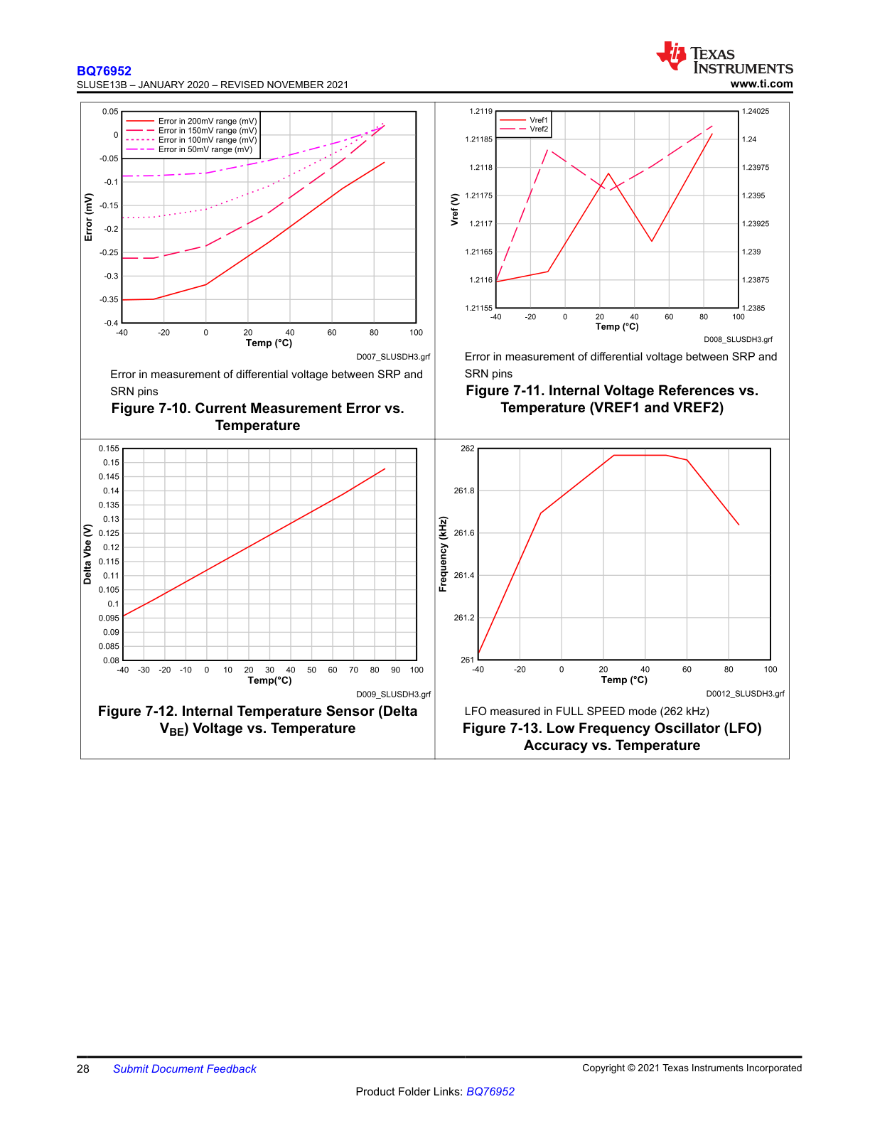
| 28 | Current, reference, temperature, and LFO characteristic plots | bq76952-p28.png |
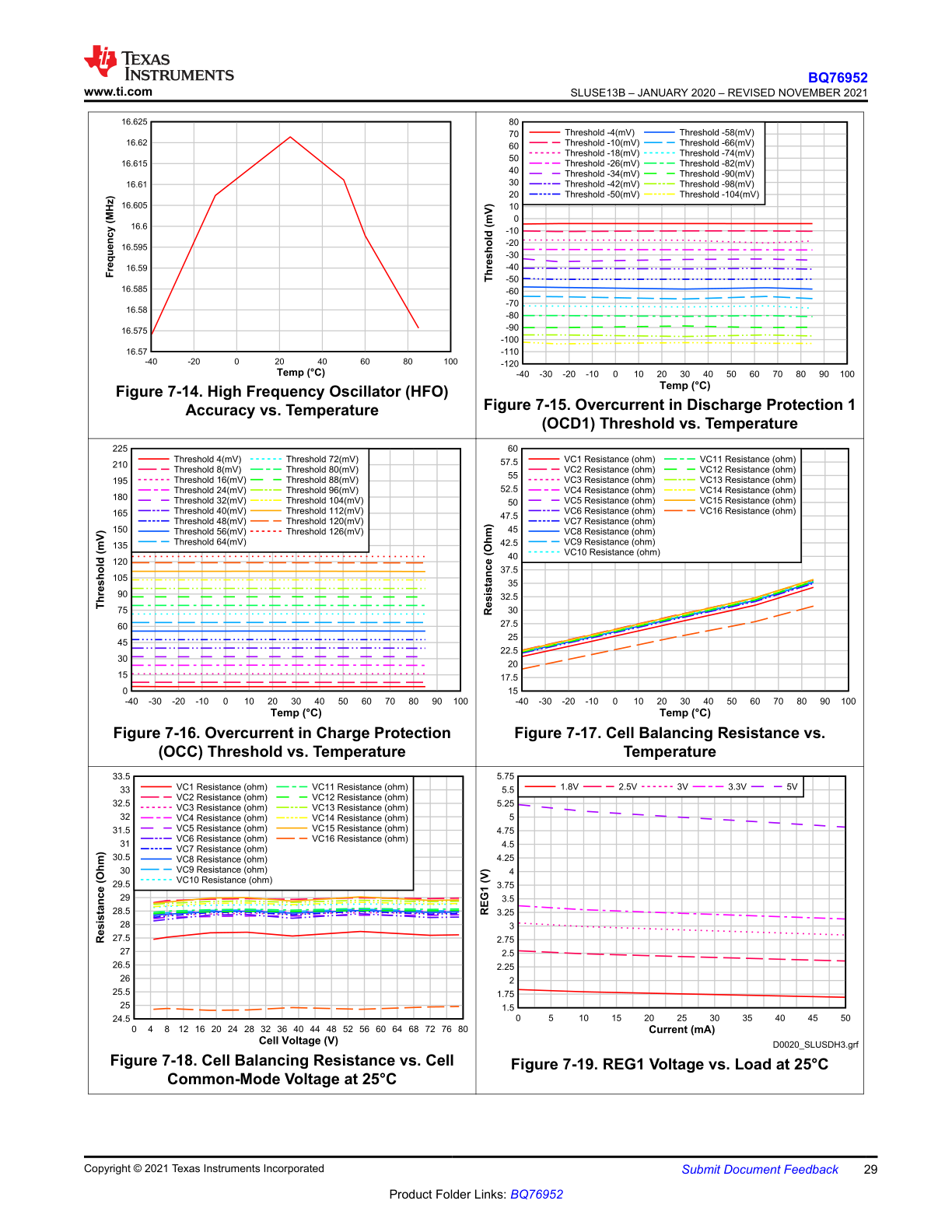
| 29 | HFO, overcurrent, balancing, and REG1 characteristic plots | bq76952-p29.png |
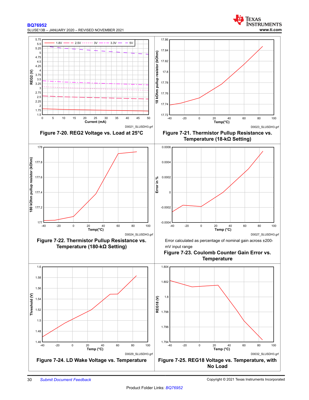
| 30 | REG2, thermistor, coulomb counter, and REG18 characteristic plots | bq76952-p30.png |
| 31 | REG18, REGIN, and low-power current characteristic plots | bq76952-p31.png |
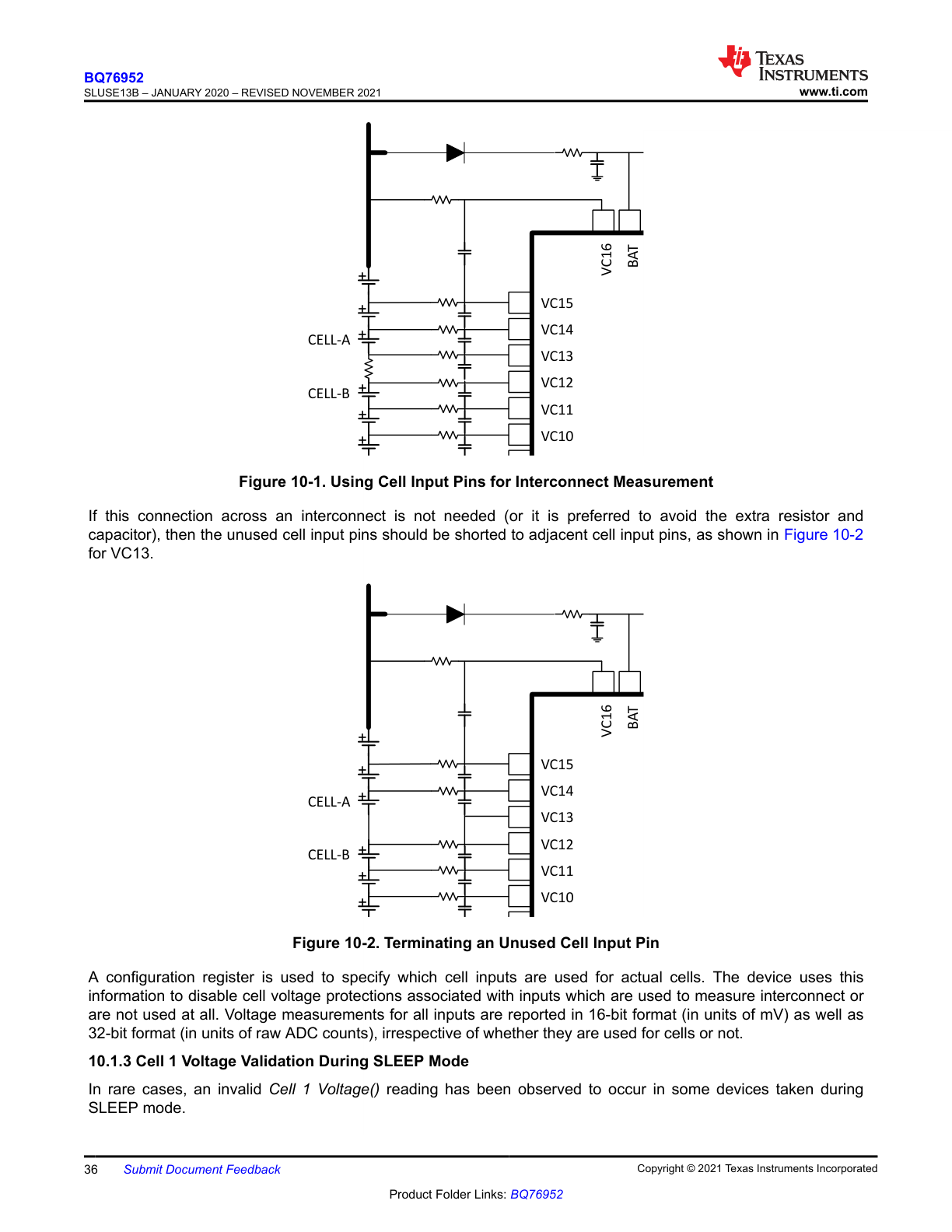
| 36 | Cell-input interconnect and unused-pin examples | bq76952-p36.png |
| 39 | External thermistor biasing example | bq76952-p39.png |
| 50 | FUSE pin operation | bq76952-p50.png |
| 51 | Device functional modes | bq76952-p51.png |
| 55 | I2C write and repeated-start read transactions | bq76952-p55.png |
| 56 | I2C read without repeated start and SPI mode timing | bq76952-p56.png |
| 58 | SPI transaction with CRC | bq76952-p58.png |
| 59 | Additional SPI CRC transaction timing | bq76952-p59.png |
| 60 | SPI transaction without CRC | bq76952-p60.png |
| 61 | Additional SPI non-CRC transaction timing | bq76952-p61.png |
| 62 | SPI transaction timing without CRC final example | bq76952-p62.png |
| 66 | 16-series typical implementation schematic page | bq76952-p66.png |
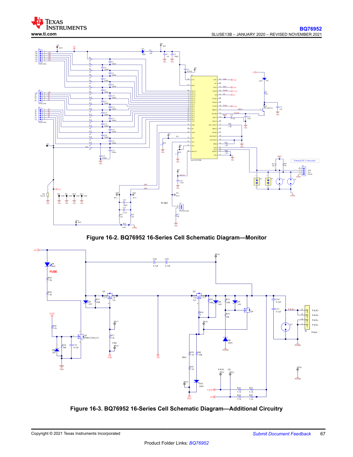
| 67 | Full 16-series monitor and additional circuitry schematics | bq76952-p67.png |
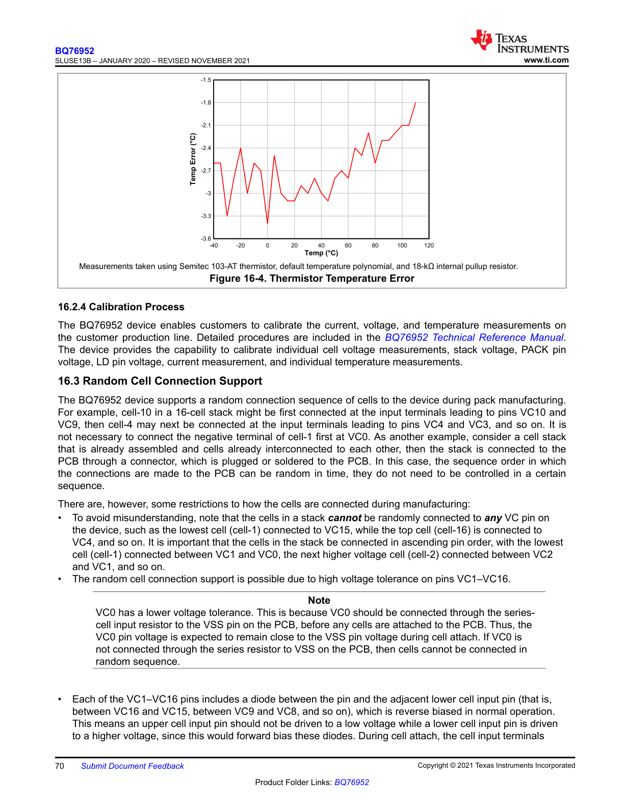
| 70 | Thermistor temperature error plot and random cell connection guidance | bq76952-p70.png |
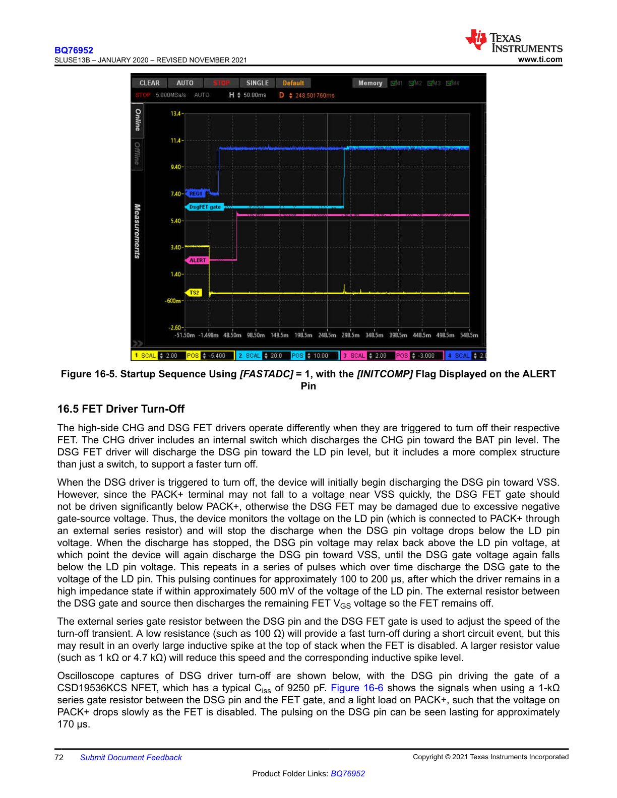
| 72 | Startup sequence timing | bq76952-p72.png |
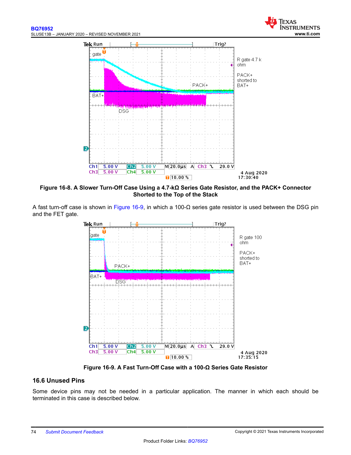
| 73 | Moderate-speed DSG FET turn-off behavior | bq76952-p73.png |
| 74 | Slow and fast DSG FET turn-off cases | bq76952-p74.png |
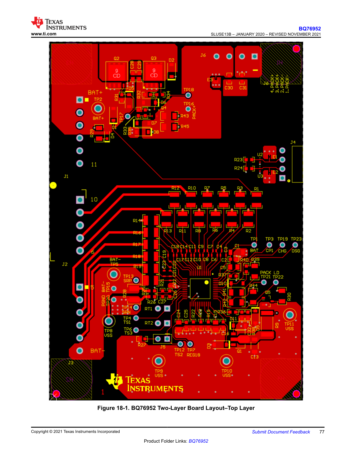
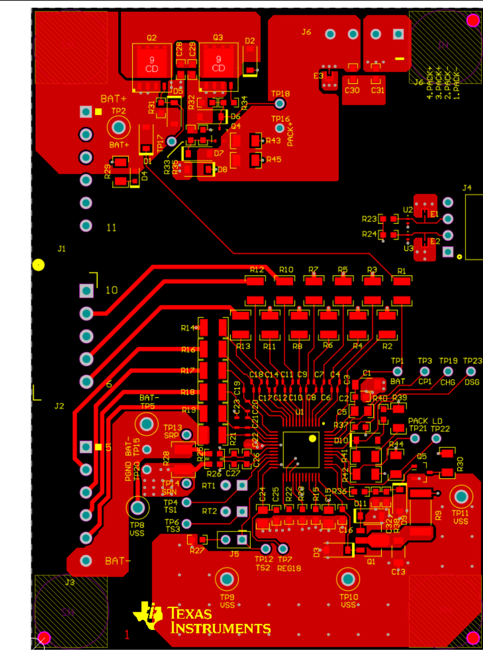
| 77 | Two-layer board layout top layer page | bq76952-p77.png |
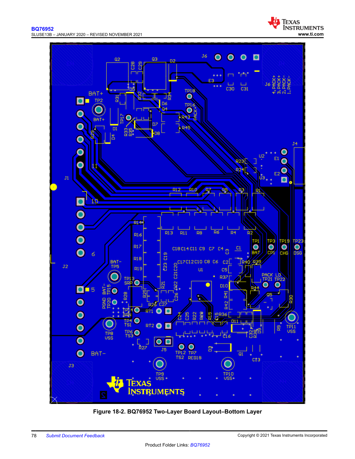
| 78 | Two-layer board layout bottom layer | bq76952-p78.png |