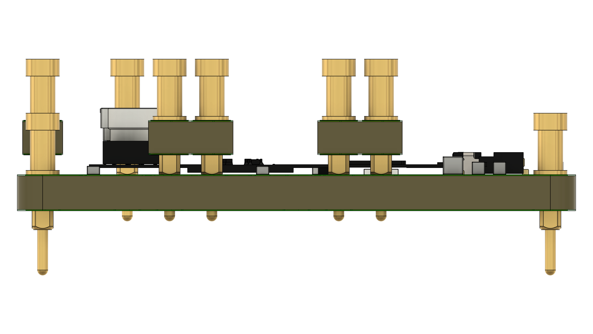
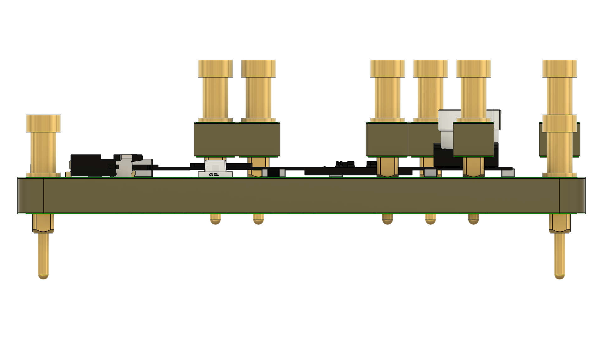
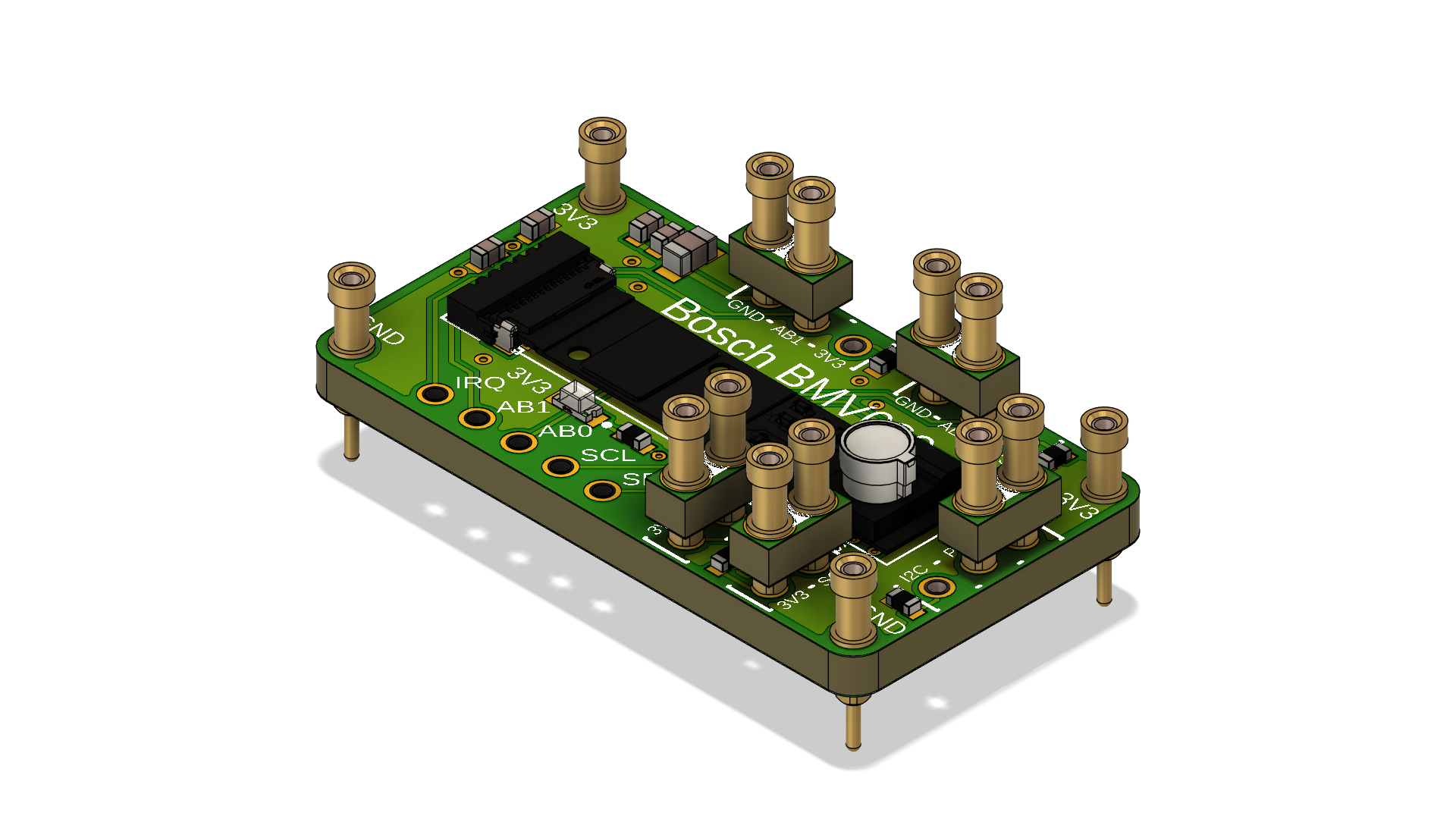
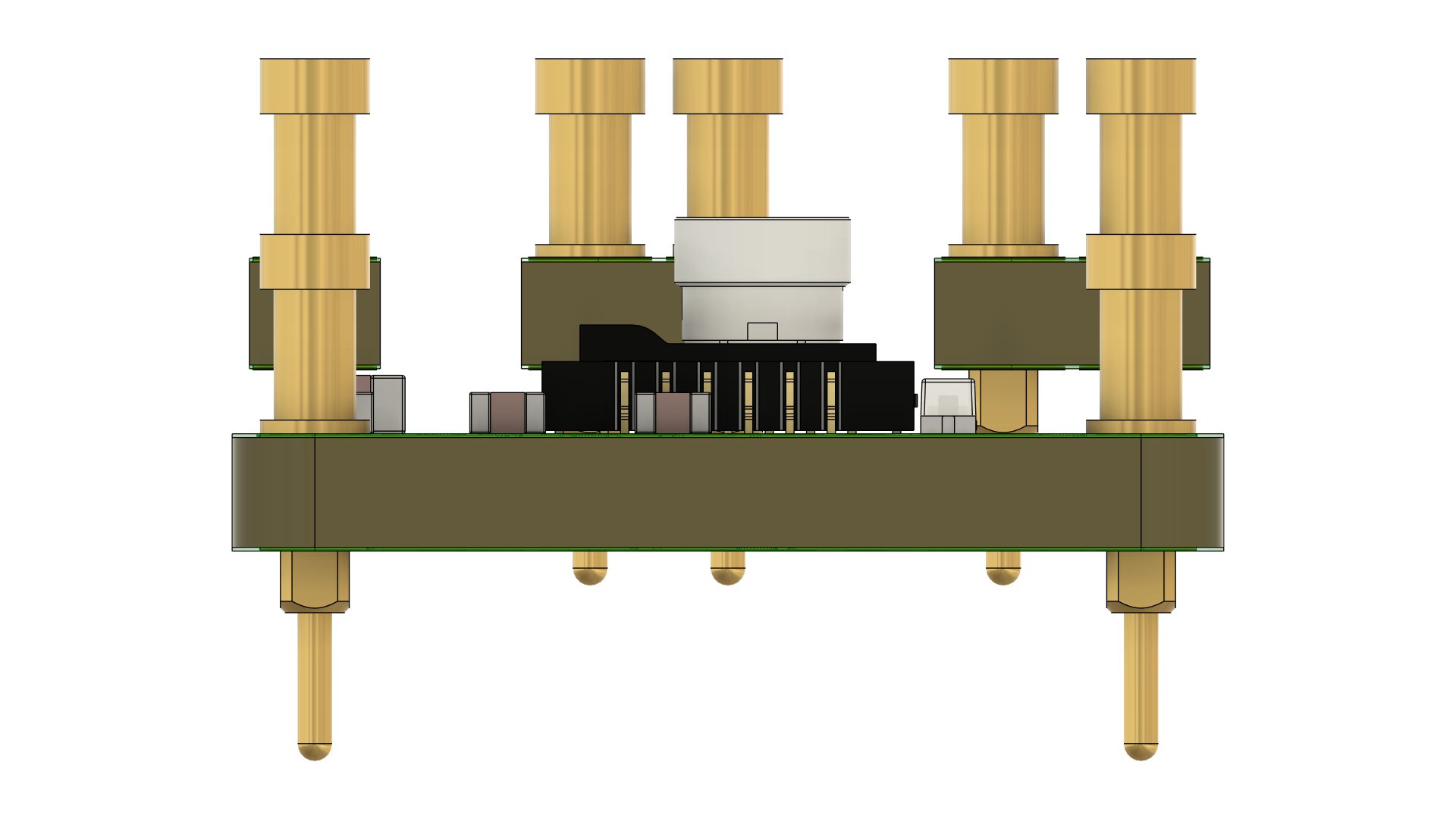
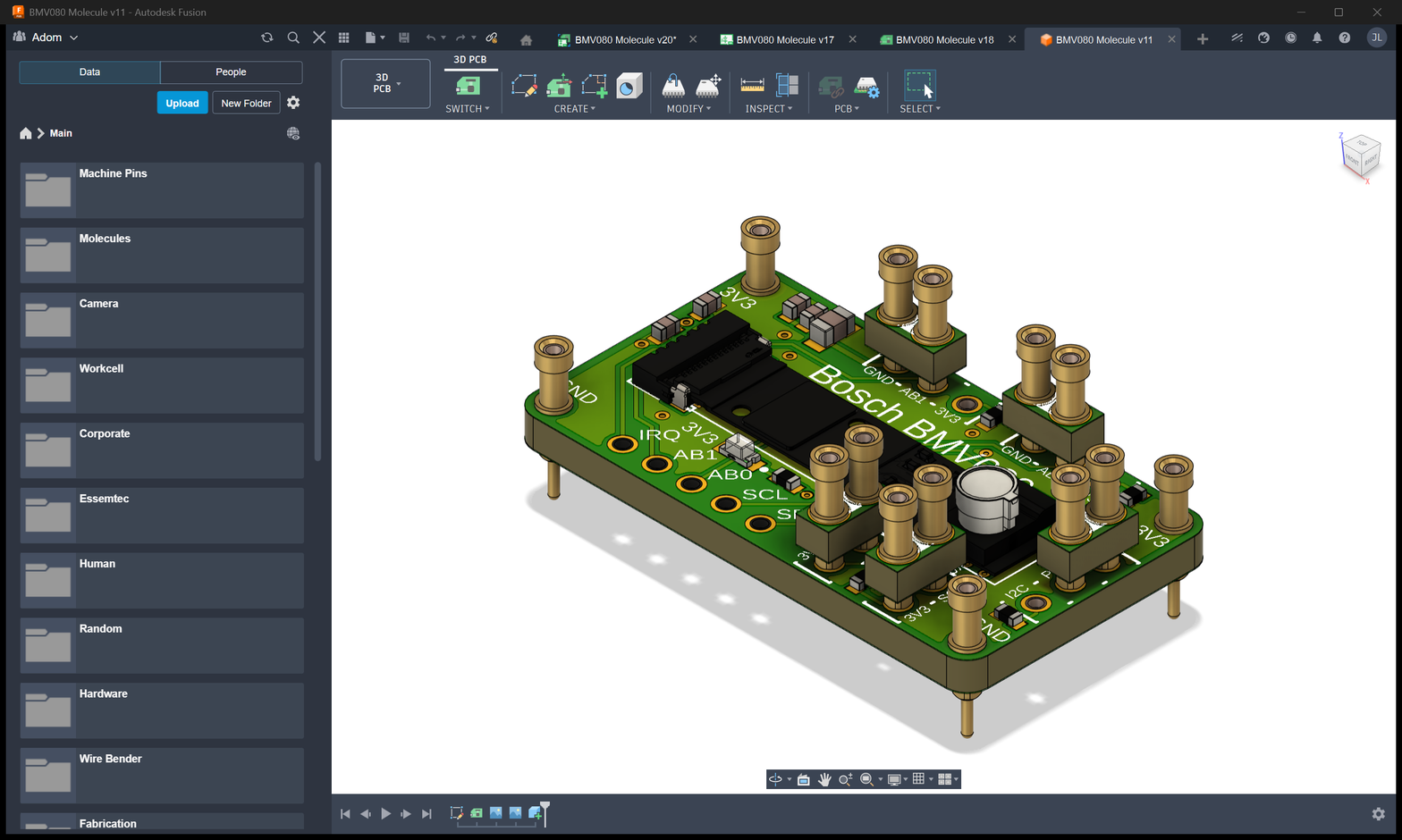
BMV080 Molecule v8
Unreviewed30×18 mm breakout for the Bosch BMV080 ultrasonic-optical particulate-matter sensor. Programmable I²C address via AB0/AB1 straps (0x54–0x57). Demo target 0x57.
BMV080 Molecule — Hardware Reference
Compact (~30×18 mm) breakout for the Bosch BMV080 ultrasonic-optical particulate-matter (PM) sensor. More elaborate than the other molecules — brings out a full configuration stack (address, interface mode, on-board pull-ups) via silk-labeled solder jumpers.
- Source: Fusion Electronics project (not on GitHub). Published assets live on the wiki.
- Wiki page: molecules/bmv080-molecule-v8-580000
- IC: BMV080 (Bosch LGA, 3.0 × 3.0 × 1.0 mm). The laser / optical block dominates the board — ~⅔ of the footprint is the sensor assembly itself.
- Silk title:
Bosch BMV080centered on top copper.
External contact map
Pin map reconstructed from the Fusion top-down render (3d-top.png on the wiki page). Four corner mount-pins at the outer corners carry power/ground, six signal pins are grouped on the bottom edge, and a row of solder-jumper pads on the top and right edges set the address and interface mode.
Corner mount-pins (power/ground)
| Position | Silk | Role |
|---|---|---|
| top-left | 3V3 |
VDDIO rail tap |
| top-right | 3V3 |
VDDIO rail tap (second tap) |
| bottom-left | GND |
Ground |
| bottom-right | GND |
Ground (second tap) |
Two independent 3V3 pins and two GND pins let you daisy-chain power in or feed separate rails for analog-vs-digital split if you want.
Bottom-edge signal pins (6 breakouts)
| Silk | Role |
|---|---|
IRQ |
Interrupt output (data ready / status) |
AB1 |
Address-select bit 1 (strapped on-board — see jumpers below) |
AB0 |
Address-select bit 0 (strapped on-board — see jumpers below) |
SCL |
I²C SCL (also SPI SCK) |
SDA |
I²C SDA (also SPI MOSI/MISO depending on mode) |
| (extra — check silk on physical board) | Likely CSB or RST |
Top-edge address-strap jumpers (silk shows 2× 3-pad [GND, ABn, 3V3] groups)
| Jumper | Silk | Bridge to set |
|---|---|---|
| AB0 strap | GND — AB0 — 3V3 |
Left bridge = AB0 low; right bridge = AB0 high |
| AB1 strap | GND — AB1 — 3V3 |
Left bridge = AB1 low; right bridge = AB1 high |
Bosch BMV080 I²C address is a 2-bit-programmable slave address (0x54–0x57) set by {AB1, AB0}. Demo firmware target is 0x57 (AB1 = AB0 = 1) — bridge both AB0 and AB1 to their 3V3 side.
Right-edge interface-mode selector (silk SPI, CS, I2C)
A 3-way jumper stack on the right edge selects the serial interface:
| Bridge | Mode |
|---|---|
I2C (bottom) |
I²C (demo target) — CSB tied high internally; SDA/SCL are the active lines |
CS (middle) |
Provides chip-select access for SPI use (shorts CSB to an external pad) |
SPI (top) |
4-wire SPI — the MISO/MOSI/SCK/CSB pads are active |
Bridge only the I2C jumper for the demo.
Bottom-middle I²C-pull-up jumpers
Silk block labeled I2C PULLUPS with two 3-pad groups: 3V3 — SDA and SCL — 3V3. Bridging each group connects the bus lines to 3V3 through on-board pull-up resistors, so you don't need external pull-ups on the SDA/SCL lines.
| Jumper | Bridged = | Behavior |
|---|---|---|
3V3 — SDA |
on-board SDA pull-up enabled | Skip the RM2's pull-up (or add-parallel — harmless) |
SCL — 3V3 |
on-board SCL pull-up enabled | Same |
For the stationary RM2 demo, the carrier already supplies external 4.7 kΩ pull-ups, so leave both of these jumpers open (or bridged — not harmful, just stacks resistance in parallel).
I²C address strap (summary for demo)
| AB1 | AB0 | Address |
|---|---|---|
| GND | GND | 0x54 |
| GND | 3V3 | 0x55 |
| 3V3 | GND | 0x56 |
| 3V3 | 3V3 | 0x57 (demo firmware target) |
Bridge both AB0 and AB1 to their 3V3 pads.
Power
| Rail | Voltage | Source |
|---|---|---|
| 3V3 (VDDIO) | 1.62–3.6 V | Host via either top corner 3V3 pin (3.3 V in demo) |
| VDD_CORE | 1.62–1.98 V | Generated on-board? — or fed externally via a dedicated 1.8 V pin if present (datasheet requires 1.8 V core + ≤ 3.3 V VDDIO) |
Datasheet: 28 mA active during measurement — much higher than any other sensor on the stationary bus (BMP581 is 70 µA, BME690 peaks at 2 mA). The +3.3V rail needs to tolerate a 28 mA pulsed load; the stationary RM2's AP2112K-3.3 LDO is rated for 600 mA so it's well within spec, but anyone cloning this onto a battery-powered carrier should budget accordingly.
Interrupts
IRQ (push-pull) asserts when a PM measurement is ready or when the sensor raises a status event. The BMV080 driver in firmware/sensors/bmv080.c currently uses polled reads, so IRQ can be left unconnected.
Wiring to the Stationary RM2 I²C bus
BMV080 3V3 (top-left or top-right)  ──── RM2 +3V3
BMV080 GND (bottom-left or bottom-right)── RM2 GND
BMV080 SDA                          ──── RM2 GPIO4 (I²C0 SDA)
BMV080 SCL                          ──── RM2 GPIO5 (I²C0 SCL)
BMV080 IRQ                          ──── (optional)
BMV080 AB0 pad / AB1 pad            ──── (leave floating — set via jumpers)
Bridge the I2C jumper (right-edge stack). Bridge both AB0 and AB1 to their 3V3 sides. Leave the I2C PULLUPS jumpers open (RM2 carrier has external pull-ups).
Gotchas for firmware bring-up
- Address-strap jumpers default to open — an unset AB0/AB1 gives a floating, indeterminate address. Bridge both to
3V3before powering. - Interface-mode jumper must be on
I2C. Factory-default is open — the chip will not respond on either interface until one of the three pads is bridged. - BMV080 needs the proprietary Bosch SDK (
lib_bmv080.a+lib_postProcessor.a) to run — vendored infirmware/sensors/bmv080_sdk/. All measurement and calibration is internal to the SDK. - 28 mA during active measurement — a lot for one sensor. Not a problem on the RM2 3V3 rail (LDO rated 600 mA) but noteworthy.
- Sensor is optical — laser / photodiode block. Handle with care; don't touch the optical window.
- If the sensor is unresponsive: the most likely culprit is the interface-mode jumper, then the address-strap jumpers, then pull-ups. The probe path is in that order.
Known gaps in this doc
Same as BME690: the .fsch/.fbrd Fusion source files are attached to the wiki page but the wiki returns 404 on design-file downloads. Silk labels and jumper positions were read from the published top-down render (3d-top.png). Exact pad coordinates, the sixth bottom-edge signal pin label, and the default/factory jumper state could not be verified without the source. If you own the Fusion project, export to .kicad_* or .sch/.brd and drop it under /bosch-molecules/BMV080/ for a full netlist extraction.