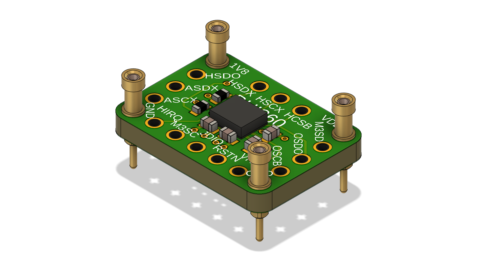
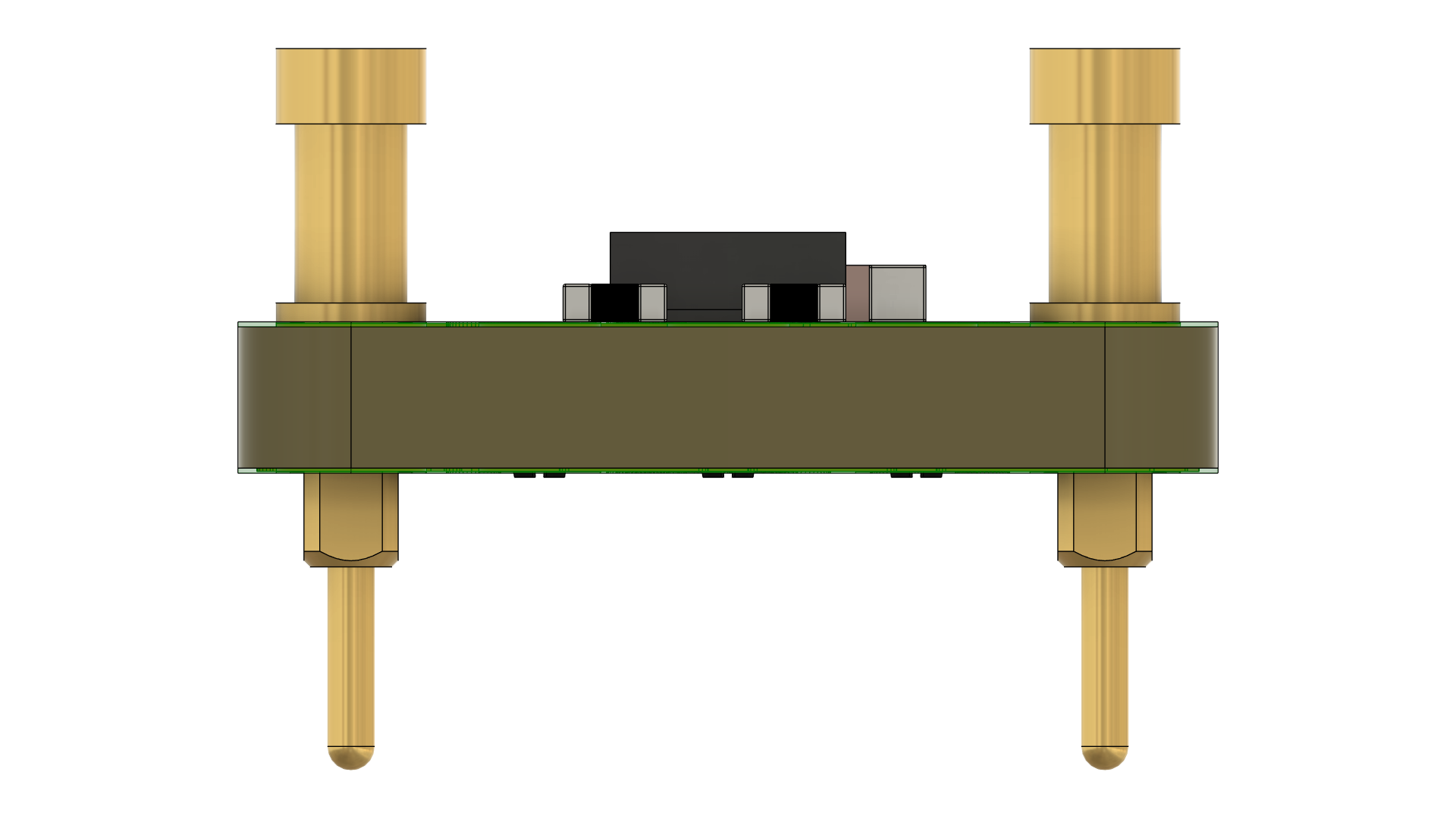
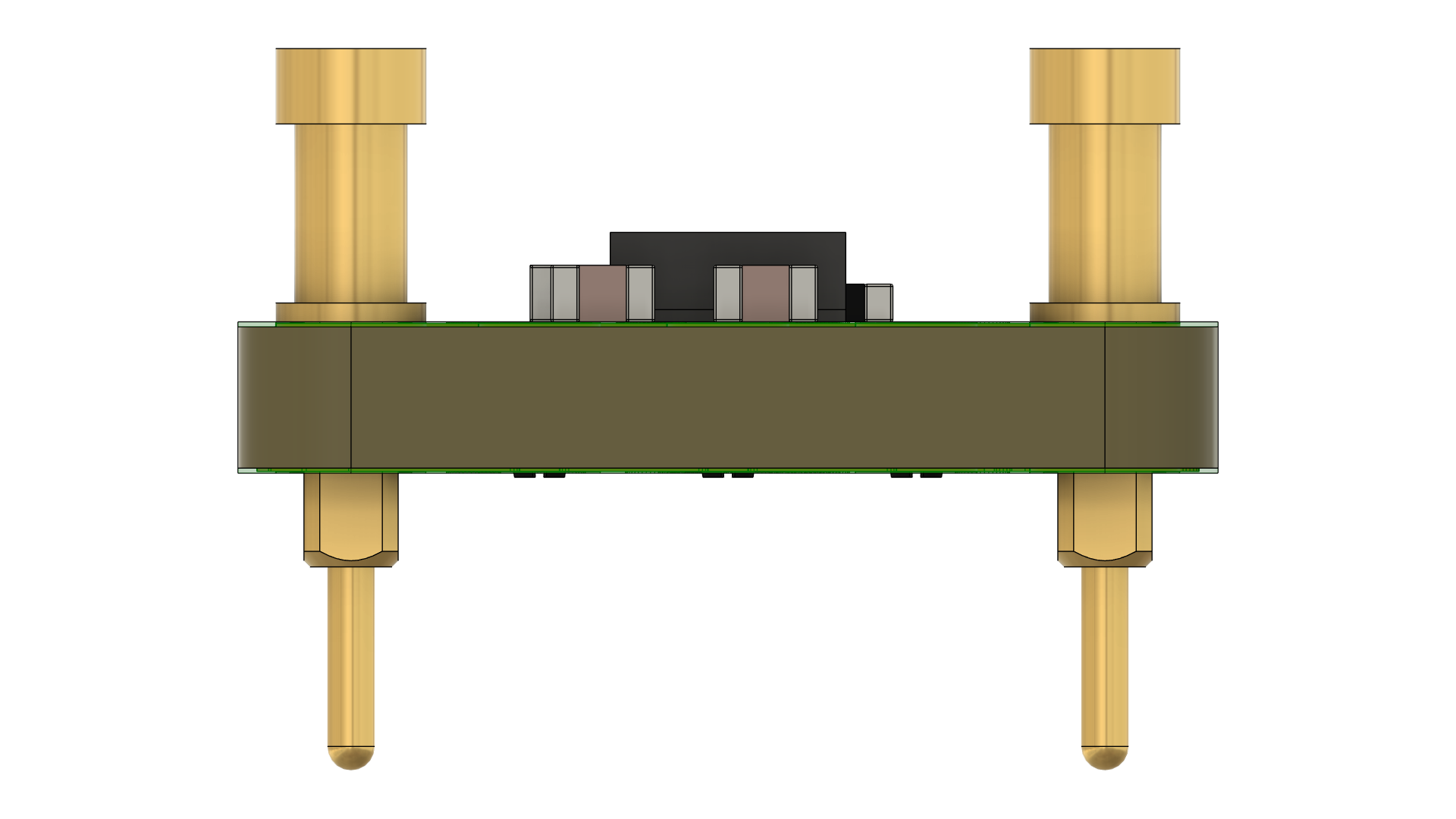
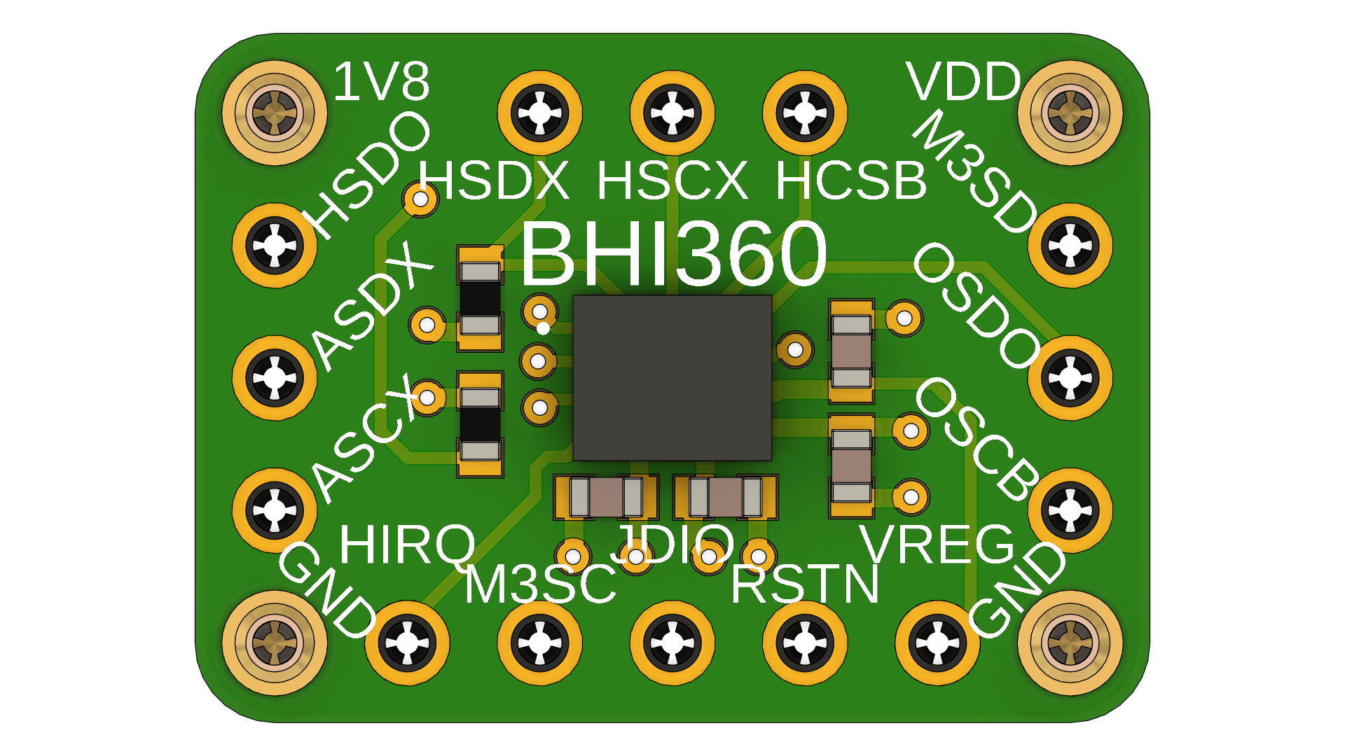
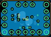
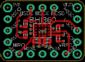
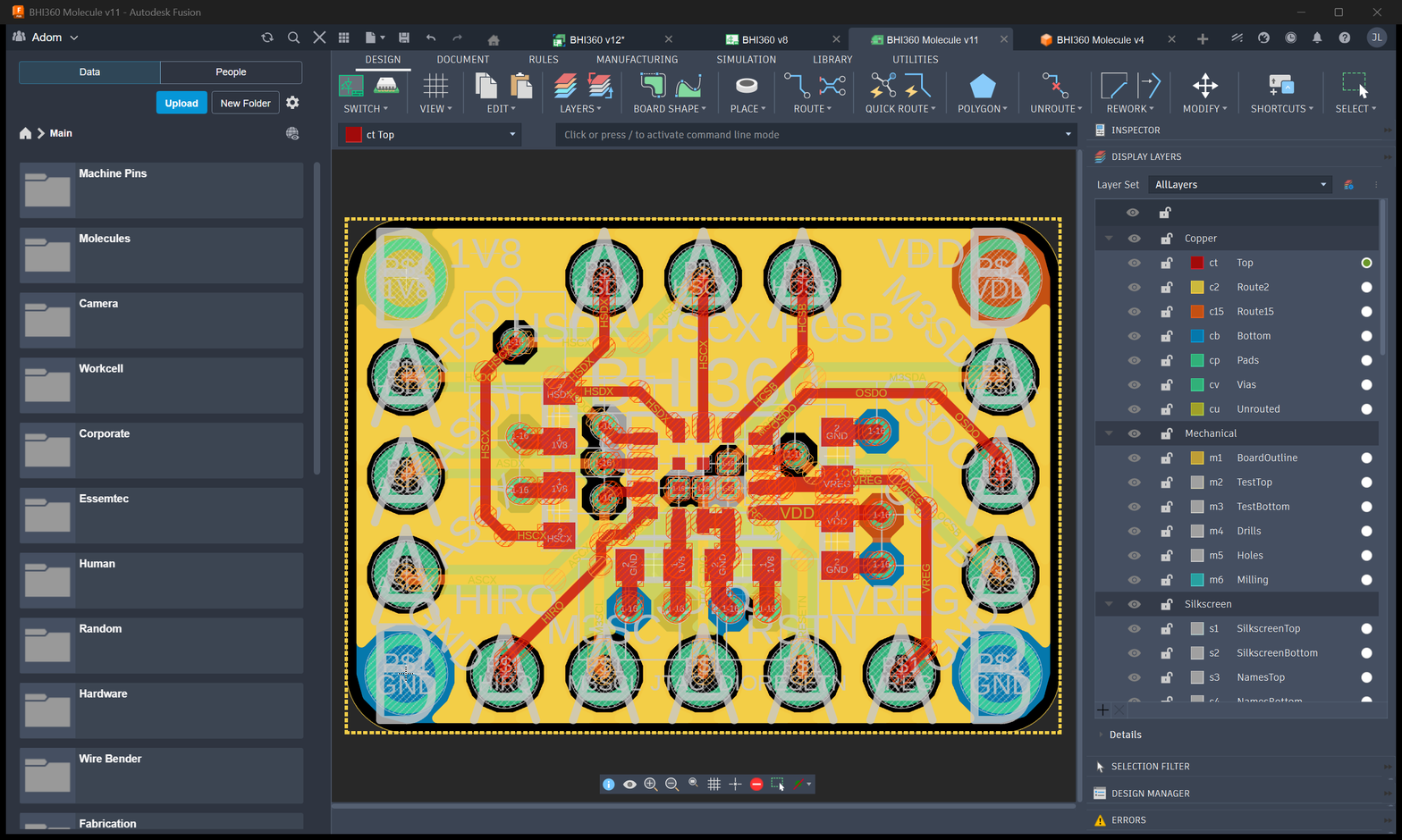
BHI360 Molecule v11
Unreviewed16×16 mm BHI360 + BMM350 combo breakout (9-DOF fusion hub + aux-bus mag). I²C at 0x28 via MC12↔MC3 strap. Runs Shuttle3 BHI360+BMM350C fusion firmware.
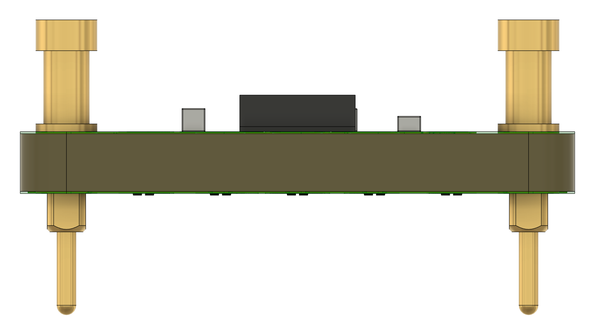
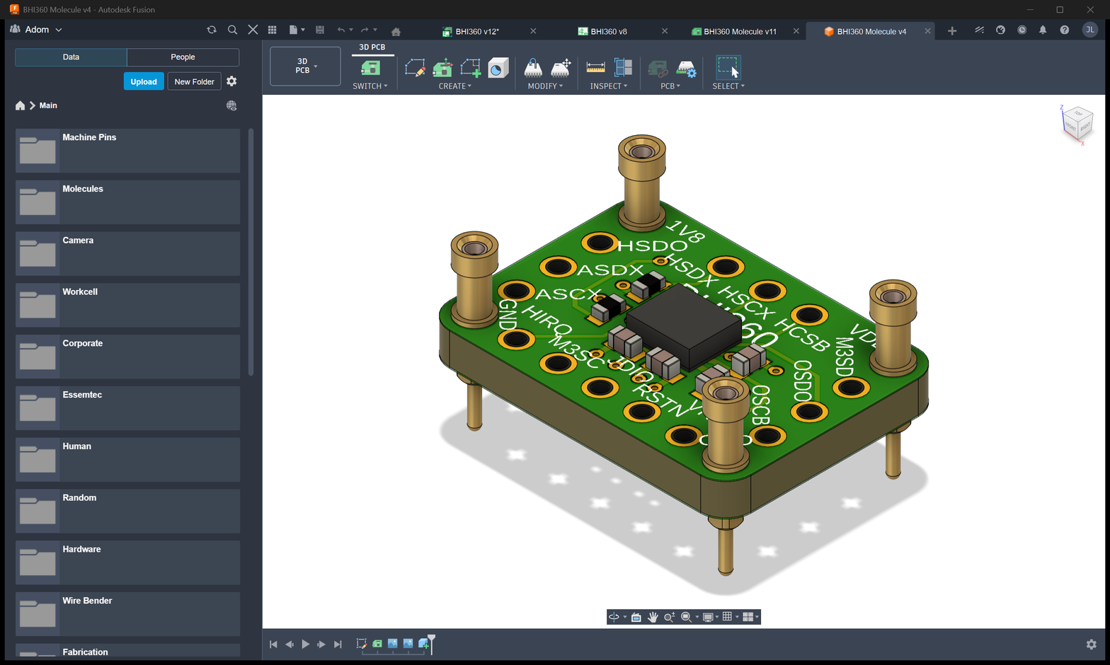
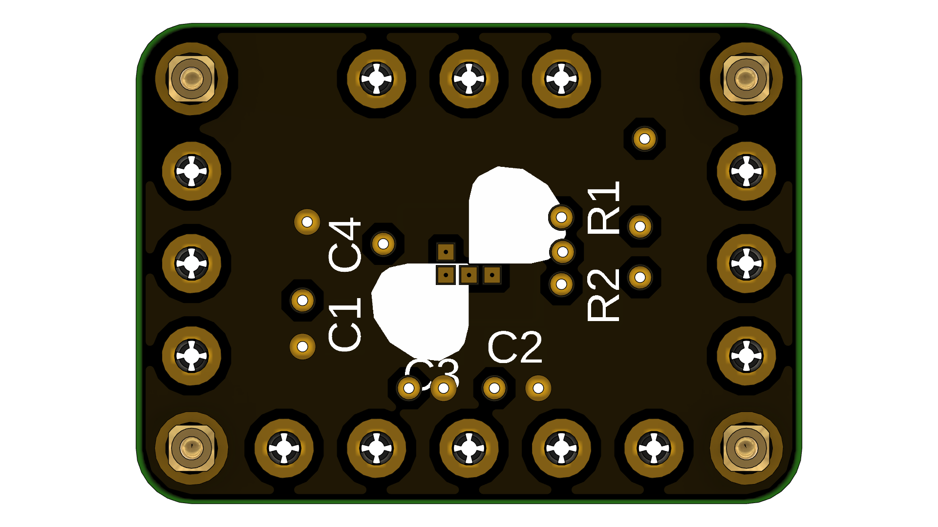
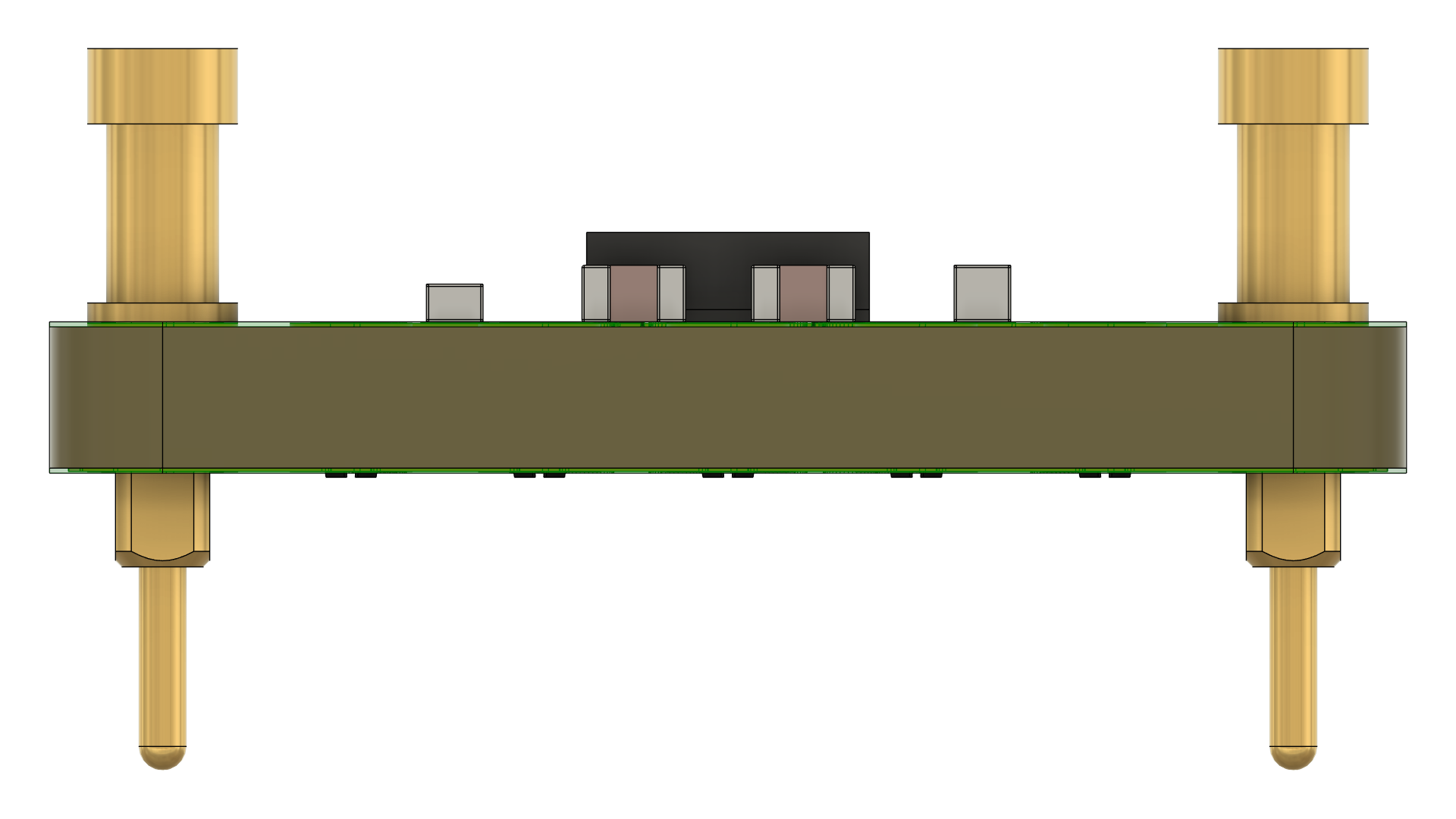
3D Model
BHI360 + BMM350 Combo Molecule — Hardware Reference
16×16 mm combo breakout carrying a Bosch BHI360 smart-sensor hub (9-DOF fusion engine) and a BMM350 magnetometer on the BHI's internal auxiliary I²C bus. This is the target board for fw_arm's BHI360 combo sensor (sensor_id 0x30 in the wire protocol).
- Source: adom-inc/bosch-molecules/Molecule_BHI360-BMM350_bosch_v1 — imported 2026-04-17
- KiCad project:
Molecule_BHI360-BMM350_bosch_v1.kicad_pro - Wiki page: molecules/bhi360-molecule-v11-137000
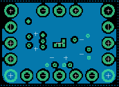
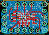
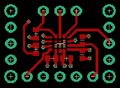
- Board: 17 contacts on two columns (X=144 west, X=160 east), single-sided, silk revision
V1: 2025-09-03, silkscreen titleBHI360+BMM350 - ICs: U1 = BHI360 (Bosch LGA-20, 2.5 × 3.0 × 0.95 mm), U2 = BMM350 (Bosch BGA-9 WLCSP)
Mechanical/electrical twin: the
Molecule_BHI385-BMM350board is identical in layout and component placement. The only difference between the two is the IC itself (BHI360 vs BHI385) and the address strap the end user should apply. If a pair of combo modules is unlabelled, trust the silkscreen title (BHI360+BMM350vsBHI385+BMM350) and the date stamp.
Component summary
| Ref | Part | Function |
|---|---|---|
| U1 | BHI360 | Smart-sensor hub — ARM Cortex-M4, runs Bosch fusion firmware |
| U2 | BMM350 | 3-axis magnetometer on U1's aux I²C bus — not on the external bus |
| C1, C5 | 100 nF 0402 | VDDIO decoupling |
| C2, C6 | 100 nF 0402 | VDD decoupling |
| C3 | VREG bypass (0603) | BHI360 internal regulator |
| C4 | 2.2 µF 0805 | BMM350 CRST reset cap |
| R1 | 10 kΩ 0402 | HCSB default pull-up to +VDDIO (holds I²C mode) |
| R2 | 10 kΩ 0402 | BMM aux-bus SCK pull-up to +VDDIO |
| R3 | 10 kΩ 0402 | BMM aux-bus SDA pull-up to +VDDIO |
| R4 | LED current-limit 0402 | For D1 (BHI_LED) |
| R5 | 10 kΩ 0402 | Default pull-up on MC12 strap → +VDDIO |
| D1 | LED 0402 | Activity LED driven by BHI_LED pin (programmable via firmware) |
External contact map
West edge (X=144)
| Ref | Silk | Net | Role |
|---|---|---|---|
| MP3 | +VDD |
+VDD |
BHI core rail — 1.71–1.89 V (1.8 V only) |
| MC6 | JTDIO |
BHI_JTSG_DIO |
JTAG data I/O — for factory debug, leave floating |
| MC1 | RST |
BHI_RST |
Active-low external reset — leave floating or pull high |
| MC10 | GND |
GND |
Ground tap |
| MC7 | M3SDA |
BHI_M3SDA |
Cortex-M3 debug SDA — leave floating |
| MC8 | M3SCL |
BHI_M3SSCL/JTAG_CLK |
Cortex-M3 debug SCL / JTAG clock — leave floating |
| MC14 | HCSB |
BHI_HCSB |
Interface strap — default high via R1 (I²C mode) |
| MC9 | SPI |
GND |
SPI-select strap — bridge MC14 ↔ MC9 to pull HCSB low (forces SPI) |
| MP1 | GND |
GND |
Ground |
East edge (X=160)
| Ref | Silk | Net | Role |
|---|---|---|---|
| MP2 | +VDDIO |
+VDDIO |
Logic rail — 1.72–3.6 V |
| MC2 | HIRQ |
BHI_HIRQ |
BHI host interrupt (active-low by default) |
| MC5 | HSCL |
BHI_HSCX |
I²C SCL to the BHI |
| MC4 | HSDA |
BHI_HSDX |
I²C SDA to the BHI |
| MC12 | 0x28 |
(floating, pulled up by R5) | Address strap — bridge MC12↔MC3 to select 0x28 |
| MC3 | HSDO |
BHI_HSDO/0x29/0x28 |
SDO / address-select pin of the BHI |
| MC14 | HCSB |
(see west) | (listed on west, repeated here for reference) |
| MC11 | 0x29 |
GND |
Address strap — bridge MC11↔MC3 to select 0x29 |
| MP4 | GND |
GND |
Ground |
I²C address strap (critical)
The BHI360's I²C slave address is set by HSDO at power-up. On this molecule, HSDO (MC3) is routed between two strap pads:
| Strap | HSDO tied to | I²C address |
|---|---|---|
Bridge MC12 ↔ MC3 (silk 0x28) |
+VDDIO (HIGH — via R5) | 0x28 ← required for this molecule |
Bridge MC11 ↔ MC3 (silk 0x29) |
GND (LOW) | 0x29 (for the BHI385 sibling molecule) |
Schematic annotation on the board: "HSDO (I2C ADD Select). Jumper to GND (LOW): 0x29. Jumper to VDDIO (HIGH): 0x28. Reset Active-LOW."
This convention is opposite to the BMI270 (where SDO→GND gives the lower address). The BHI hub uses the inverted mapping internally; don't port an address rule from BMI270 over to BHI and expect it to work.
For this BHI360 molecule: solder-bridge MC12 to MC3 so the firmware finds it at 0x28. On its sibling BHI385 molecule, bridge MC11 to MC3 for 0x29 instead.
Interface strap (HCSB — I²C vs SPI)
| HCSB state | Mode |
|---|---|
| Floating / pulled high (default via R1) | I²C |
Bridge MC14 ↔ MC9 (silk SPI) |
SPI (active-low select) |
Leave unbridged for I²C.
Aux I²C bus (BMM350 — internal)
U2 (BMM350) is wired to U1's auxiliary I²C master:
| BMM350 pin | U1 (BHI360) pin |
|---|---|
| SDA (A2) | BHI M_SDA (pin 2) |
| SCK (A3) | BHI M_SCK (pin 3) |
| INT (A1) | BHI M_INT (pin 10) |
| ADSEL (B2) | GND — fixed on-board via net +VDDIO pull tap only on standalone BMM350 |
Schematic text on this molecule: "ADSEL (Legacy I2C Add): GND = 0x14" — confirms the on-board BMM350 is strapped to 0x14 on the aux bus. The BHI360 firmware blob (Bosch_Shuttle3_BHI360_BMM350C.fw) expects to find the mag at 0x14 on its aux master, so this matches.
The aux BMM350 is not visible on the external I²C lines. The host only sees the BHI hub at 0x28. Magnetometer samples come out of the BHI fusion engine as virtual-sensor outputs.
Power
| Rail | Voltage | Source |
|---|---|---|
| VDD (BHI core + BMM core) | 1.71–1.89 V | 1.8 V rail (shared with BMM350 and BHI385 VDD) |
| VDDIO (both ICs) | 1.72–3.6 V | Host 3.3 V via MP2 |
Schematic annotation: "BHI360: VDD 1.71–1.89 V, VDDIO 1.72–3.6 V, Turbo Mode 2.8 mA, Typical 0.95 mA." Typical active current for the hub alone is ~0.95 mA, peaking at 2.8 mA during firmware RAM upload / turbo mode.
Firmware upload
First-time boot requires the host to upload a firmware blob to the BHI360's SRAM via I²C. For this combo we use Bosch_Shuttle3_BHI360_BMM350C.fw (the Shuttle3-board fused firmware — BHI360 + BMM350 as 9-DOF virtual sensors). The blob is vendored in firmware/sensors/bhi360_sdk/Bosch_Shuttle3_BHI360_BMM350C.fw.h.
Upload flow (already wired in fw_arm):
- Host sends
UPLOAD_BEGINframe (sensor_id 0x30, blob size, CRC32). - Arm RM2 calls
bhy2_upload_firmware_to_ram()(Bosch BHY2 SDK) over I²C. - Host streams
UPLOAD_CHUNKframes. - Host sends
UPLOAD_END; arm responds withUPLOAD_STATUScontaining CRC check result. - Firmware boots from RAM and the BHI360 starts exposing virtual-sensor IDs (accel, gyro, mag, orientation, rotation vector, gesture detectors, etc.).
Interrupt + LED
- HIRQ (MC2): BHI → host interrupt line. Active-low. Signals FIFO not empty or async events. The
fw_armBHI driver polls by default, so wiring HIRQ is optional, but pulling in HIRQ enables efficient low-latency FIFO draining. - LED (D1): driven off-board by the BHI's LED pin; programmable via firmware. Useful "is the chip alive?" indicator during bring-up.
Wiring to the Arm RM2 I²C bus
Combo MP3 (VDD)  ──── +1.8 V rail
Combo MP2 (VDDIO)──── RM2 +3V3
Combo MP1 (GND)  ──── RM2 GND       (MP4 is a second GND tap — parallel OK)
Combo MC4 (HSDA) ──── RM2 GPIO4 (I²C0 SDA, shared bus)
Combo MC5 (HSCL) ──── RM2 GPIO5 (I²C0 SCL, shared bus)
Combo MC2 (HIRQ) ──── (optional GPIO; enables IRQ-driven FIFO drain)
Combo MC1 (RST)  ──── (optional GPIO, or tie to +VDDIO through 10 kΩ)
Solder-bridge MC12 ↔ MC3 (strap to VDDIO / silk 0x28).
Leave unconnected: MC6 (JTDIO), MC7 (M3SDA), MC8 (M3SCL), MC9 (SPI), MC11 (0x29 strap), MC14 (HCSB).
Gotchas for firmware bring-up
- Address strap is non-obvious and non-standard. Bridge MC12↔MC3 on the BHI360 board (gives 0x28). The silk label "0x28" is on MC12 and the board's behavior depends on you actually making that bridge.
- VDD = 1.8 V only (shared with the BHI385 and standalone BMM350).
- No external I²C pull-ups on this molecule — rely on the main bus pull-ups. R2/R3 are on the internal aux bus, not the external bus.
- RST (MC1) is active-low. If you wire it up, default it high. Never drive it high; use an open-drain driver or tie to +VDDIO via 10 kΩ.
- Firmware blob upload takes ~1–2 seconds — during that window, no other I²C traffic should hit this sensor. The
fw_armdispatcher enforces this with aSELECTlock. - Aux BMM350 is captive to U1's fusion engine — you cannot talk to it directly. If you need raw magnetometer data at non-fused rates, use the standalone BMM350 molecule on the same bus at 0x15.
- The JTAG / M3 contacts (MC6, MC7, MC8) are for Bosch factory debug. Do not connect them to GPIOs in the demo. Leave floating.