ATmega328P — 8-bit AVR Microcontroller
UnreviewedMicrochip (Atmel) ATmega328P. 8-bit AVR RISC, 32KB flash, 2KB SRAM, 1KB EEPROM, 23 I/O, 10-bit ADC, 20 MHz, 1.8–5.5 V. The core of the Arduino Uno.
Source: Microchip / Atmel Datasheet (DS40002061B)
Manufacturer: Microchip (formerly Atmel)
Part Number: ATmega328P
Document: DS40002061B — 2020 (megaAVR, part of ATmega48A/PA/88A/PA/168A/PA/328/P family datasheet)
Architecture: 8-bit AVR RISC
Description
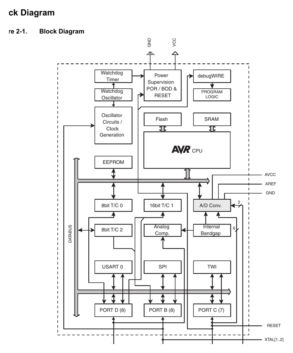
The ATmega328P is a low-power CMOS 8-bit microcontroller based on the AVR enhanced RISC architecture. By executing powerful instructions in a single clock cycle, it achieves throughputs approaching 1 MIPS per MHz, allowing the system designer to optimize power consumption versus processing speed. The ATmega328P combines 32 KB of ISP flash with read-while-write capabilities, 1 KB EEPROM, 2 KB SRAM, 23 general-purpose I/O lines, 32 general-purpose working registers, three flexible timer/counters with compare modes, internal and external interrupts, a serial programmable USART, a byte-oriented 2-wire serial interface, an SPI serial port, a 6-channel 10-bit ADC (8 channels in TQFP and QFN/MLF packages), a programmable watchdog timer with internal oscillator, and five software-selectable power-saving modes. This part is the microcontroller at the heart of the Arduino Uno / Nano / Pro Mini.
Key Specifications
| Parameter | Value |
|---|---|
| Architecture | 8-bit AVR RISC |
| Flash Memory | 32 KB (ISP, read-while-write) |
| SRAM | 2 KB |
| EEPROM | 1 KB |
| Operating Voltage | 1.8 V – 5.5 V |
| Max Clock | 20 MHz @ 4.5 V – 5.5 V |
| Max MIPS | 20 MIPS @ 20 MHz |
| Digital I/O Lines | 23 |
| ADC | 10-bit, 8-channel (TQFP/VQFN), 6-channel (SPDIP) |
| Timers | 2 × 8-bit + 1 × 16-bit, PWM channels ×6 |
| Serial Interfaces | USART, SPI, 2-wire (I²C-compatible) |
| Interrupt Sources | 26 |
| Temperature Range | −40 °C to 85 °C (industrial); −40 °C to 105 °C (extended) |
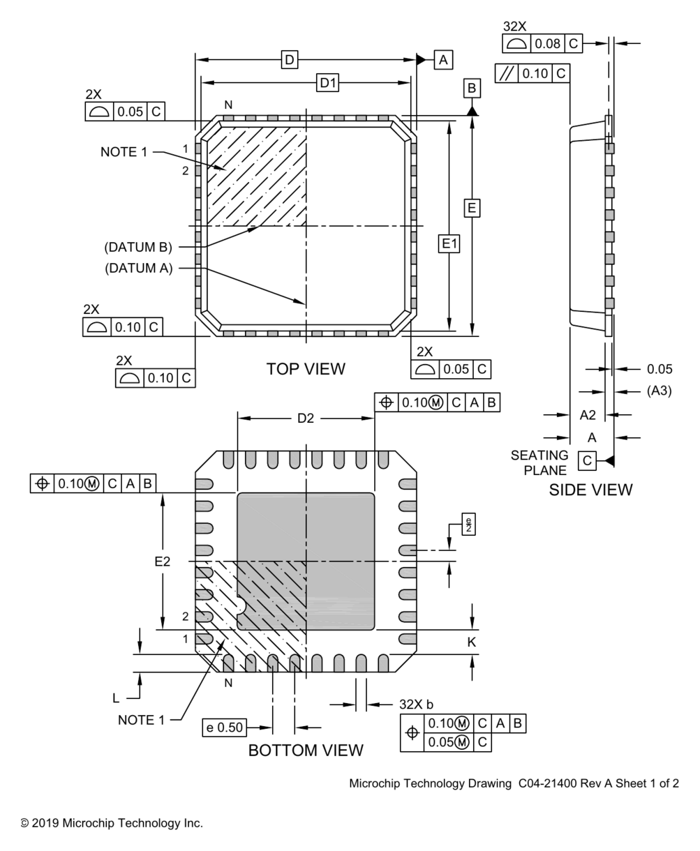
| Packages | 28-pin PDIP, 32-pin TQFP, 28-pad VQFN, 32-pad VQFN |
| Active Current @ 8 MHz, 5 V | 5.2 mA typ |
| Power-down Current @ 3 V | 0.1 µA typ |
Features
- High-performance, low-power AVR 8-bit microcontroller
- Advanced RISC architecture — 131 instructions, mostly single-cycle execution, 32 × 8 general-purpose working registers, fully static operation, up to 20 MIPS throughput at 20 MHz, on-chip 2-cycle multiplier
- High-endurance non-volatile memory — 32 KB in-system self-programmable flash, 1 KB EEPROM, 2 KB internal SRAM; 10 000 flash / 100 000 EEPROM write-erase cycles; 20-year data retention at 85 °C / 100 years at 25 °C
- Optional boot-loader section with independent lock bits; in-system programming via the on-chip boot program; true read-while-write operation
- Programming lock for software security
- QTouch library support: capacitive touch buttons, sliders and wheels; up to 64 sense channels
- Peripheral features — Two 8-bit timer/counters and one 16-bit timer/counter with separate prescaler, compare & capture modes; real-time counter with separate oscillator; six PWM channels; 10-bit 6-channel ADC (SPDIP) or 8-channel ADC (TQFP/QFN) with optional temperature measurement; programmable serial USART; master/slave SPI; byte-oriented 2-wire serial (Philips I²C compatible); programmable watchdog timer with separate on-chip oscillator; on-chip analog comparator; interrupt & wake-up on pin change
- Special microcontroller features — Power-on reset and programmable brown-out detection; internal calibrated RC oscillator; external and internal interrupt sources; six sleep modes: Idle, ADC noise reduction, Power-save, Power-down, Standby, Extended Standby
- I/O and packages — 23 programmable I/O lines; 28-pin SPDIP, 32-lead TQFP, 28-pad VQFN, 32-pad VQFN
- Operating voltage: 1.8 V – 5.5 V
- Temperature range: −40 °C to 85 °C (industrial), extended to −40 °C to 105 °C on select orderable codes
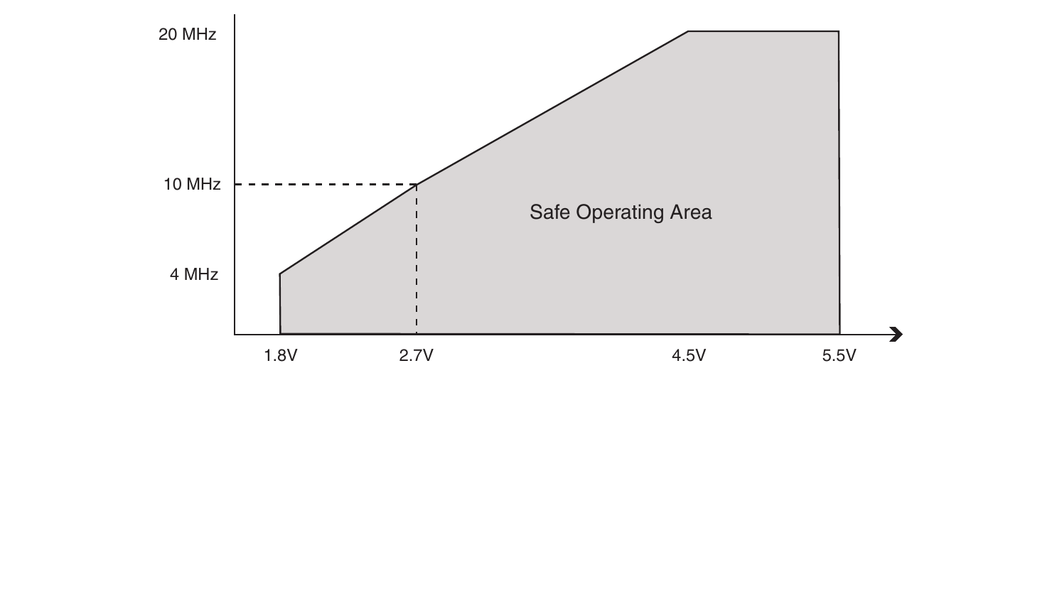
- Speed grades: 0 – 4 MHz @ 1.8 – 5.5 V, 0 – 10 MHz @ 2.7 – 5.5 V, 0 – 20 MHz @ 4.5 – 5.5 V
- Ultra-low power: 0.2 mA active @ 1 MHz / 1.8 V / 25 °C; 0.1 µA power-down; 0.75 µA power-save (32 kHz RTC on)
Pin Configuration
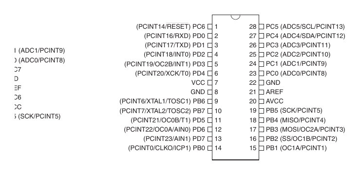
Pinout shown for the 28-pin SPDIP / 28-pad VQFN package. The 32-pin TQFP / VQFN adds two extra ADC channels (ADC6, ADC7) and separate AVCC / AGND pins.
| Pin | Name | Type | Description |
|---|---|---|---|
| 1 | PC6 / RESET | I/O / Reset | Port C bit 6 when RSTDISBL fuse is programmed; otherwise active-low reset. Also PCINT14. |
| 2 | PD0 | I/O | Port D bit 0. RXD (USART input), PCINT16. |
| 3 | PD1 | I/O | Port D bit 1. TXD (USART output), PCINT17. |
| 4 | PD2 | I/O | Port D bit 2. INT0 external interrupt, PCINT18. |
| 5 | PD3 | I/O | Port D bit 3. INT1, OC2B PWM, PCINT19. |
| 6 | PD4 | I/O | Port D bit 4. XCK (USART clock) / T0 (Timer0 ext. clock), PCINT20. |
| 7 | VCC | Power | Digital supply voltage (1.8 V – 5.5 V). |
| 8 | GND | Power | Ground. |
| 9 | PB6 | I/O / XTAL1 | Port B bit 6 or crystal/resonator input XTAL1 / TOSC1. PCINT6. |
| 10 | PB7 | I/O / XTAL2 | Port B bit 7 or crystal/resonator output XTAL2 / TOSC2. PCINT7. |
| 11 | PD5 | I/O | Port D bit 5. T1 (Timer1 ext. clock), OC0B PWM, PCINT21. |
| 12 | PD6 | I/O | Port D bit 6. AIN0 (analog comparator +), OC0A PWM, PCINT22. |
| 13 | PD7 | I/O | Port D bit 7. AIN1 (analog comparator −), PCINT23. |
| 14 | PB0 | I/O | Port B bit 0. ICP1 (Timer1 input capture), CLKO (clock output), PCINT0. |
| 15 | PB1 | I/O | Port B bit 1. OC1A PWM, PCINT1. |
| 16 | PB2 | I/O | Port B bit 2. SS̄ (SPI slave select), OC1B PWM, PCINT2. |
| 17 | PB3 | I/O | Port B bit 3. MOSI (SPI data in), OC2A PWM, PCINT3. |
| 18 | PB4 | I/O | Port B bit 4. MISO (SPI data out), PCINT4. |
| 19 | PB5 | I/O | Port B bit 5. SCK (SPI clock), PCINT5. |
| 20 | AVCC | Power | ADC supply voltage. Must be within ±0.3 V of VCC; connect through LC filter when ADC is used. |
| 21 | AREF | Analog | ADC reference voltage input. |
| 22 | GND | Power | Ground (analog / digital). |
| 23 | PC0 | I/O | Port C bit 0. ADC0, PCINT8. |
| 24 | PC1 | I/O | Port C bit 1. ADC1, PCINT9. |
| 25 | PC2 | I/O | Port C bit 2. ADC2, PCINT10. |
| 26 | PC3 | I/O | Port C bit 3. ADC3, PCINT11. |
| 27 | PC4 | I/O | Port C bit 4. ADC4, SDA (TWI data), PCINT12. |
| 28 | PC5 | I/O | Port C bit 5. ADC5, SCL (TWI clock), PCINT13. |
Absolute Maximum Ratings
| Parameter | Value | Unit |
|---|---|---|
| Operating Temperature | −55 to +125 | °C |
| Storage Temperature | −65 to +150 | °C |
| Voltage on any pin (except RESET) w.r.t. GND | −0.5 to VCC + 0.5 | V |
| Voltage on RESET w.r.t. GND | −0.5 to +13.0 | V |
| Maximum Operating Voltage | 6.0 | V |
| DC Current per I/O Pin | 40.0 | mA |
| DC Current VCC and GND Pins | 200.0 | mA |
Stresses beyond these ratings may cause permanent damage. Exposure to absolute-maximum conditions for extended periods may affect device reliability.
Recommended Operating Conditions
| Parameter | Min | Typ | Max | Unit |
|---|---|---|---|---|
| Supply Voltage VCC | 1.8 | — | 5.5 | V |
| Ambient Temperature (industrial) | −40 | — | +85 | °C |
| Ambient Temperature (extended) | −40 | — | +105 | °C |
| Clock Frequency @ 1.8 – 2.7 V | 0 | — | 4 | MHz |
| Clock Frequency @ 2.7 – 4.5 V | 0 | — | 10 | MHz |
| Clock Frequency @ 4.5 – 5.5 V | 0 | — | 20 | MHz |
Electrical Characteristics
ATmega328P DC Characteristics — TA = −40 °C to 85 °C, VCC = 1.8 V to 5.5 V (unless otherwise noted).
| Symbol | Parameter | Condition | Typ | Max | Unit |
|---|---|---|---|---|---|
| ICC | Active Supply Current | 1 MHz, VCC = 2 V | 0.3 | 0.5 | mA |
| ICC | Active Supply Current | 4 MHz, VCC = 3 V | 1.7 | 2.5 | mA |
| ICC | Active Supply Current | 8 MHz, VCC = 5 V | 5.2 | 9 | mA |
| ICC | Idle Supply Current | 1 MHz, VCC = 2 V | 0.04 | 0.15 | mA |
| ICC | Idle Supply Current | 4 MHz, VCC = 3 V | 0.3 | 0.7 | mA |
| ICC | Idle Supply Current | 8 MHz, VCC = 5 V | 1.2 | 2.7 | mA |
| ICC | Power-save — 32 kHz TOSC enabled | VCC = 1.8 V | 0.8 | — | µA |
| ICC | Power-save — 32 kHz TOSC enabled | VCC = 3 V | 0.9 | — | µA |
| ICC | Power-down — WDT enabled | VCC = 3 V | 4.2 | 8 | µA |
| ICC | Power-down — WDT disabled | VCC = 3 V | 0.1 | 2 | µA |
ADC Characteristics (from Table 29-15)
| Parameter | Min | Typ | Max | Unit |
|---|---|---|---|---|
| Resolution | — | 10 | — | Bits |
| Absolute accuracy, ADC clock = 200 kHz (VREF = VCC = 4 V) | — | 2 | 4.5 | LSB |
| Integral Non-Linearity (INL) | — | 0.5 | — | LSB |
| Differential Non-Linearity (DNL) | — | 0.25 | — | LSB |
| Gain Error | — | 2 | — | LSB |
| Offset Error | — | 2 | — | LSB |
| Conversion Time (free-running) | 13 | — | 260 | µs |
| Clock Frequency | 50 | — | 1000 | kHz |
| Analog Supply Voltage AVCC | VCC − 0.3 | — | VCC + 0.3 | V |
| Reference Voltage VREF | 1.0 | — | AVCC | V |
| Internal Voltage Reference | 1.0 | 1.1 | 1.2 | V |
| Analog Input Resistance RAIN | — | 100 | — | MΩ |
Extended Temperature (TA = −40 °C to 105 °C). Active-mode ICC typicals are identical to the 85 °C table; max values increase slightly (e.g. power-down max 5 µA instead of 2 µA). See datasheet §30 for the full 105 °C characterization.
Memory Map
The ATmega328P has three separate memory spaces: program flash, data SRAM, and EEPROM.
Program Memory (Flash) — 32 KB organized as 16K × 16 (16-bit wide instructions). The Program Counter is 14 bits wide. Flash is split into an Application Flash Section and an optional Boot Flash Section; the boot section size is fuse-selectable (256/512/1024/2048 words).
| Region | Start | End | Size |
|---|---|---|---|
| Application Flash Section | 0x0000 | 0x3FFF (or BOOTSZ boundary − 1) | ≤ 32 KB |
| Boot Flash Section (optional) | BOOTSZ boundary | 0x3FFF | 0.5 – 4 KB |
Data Memory (SRAM) — 2 KB of internal SRAM plus the AVR's memory-mapped register file and I/O space.
| Region | Start | End | Size |
|---|---|---|---|
| 32 General-Purpose Registers (R0–R31) | 0x0000 | 0x001F | 32 B |
| 64 Standard I/O Registers | 0x0020 | 0x005F | 64 B |
| 160 Extended I/O Registers | 0x0060 | 0x00FF | 160 B |
| Internal SRAM | 0x0100 | 0x08FF | 2048 B |
Only ST/STS/STD and LD/LDS/LDD instructions reach the Extended I/O space (0x60–0xFF); the shorter IN/OUT opcodes only address the 64 standard I/O registers. SRAM access takes two clkCPU cycles. The stack grows downward from RAMEND (0x08FF) — user code must initialize the Stack Pointer (SPH:SPL) before any CALL/PUSH.
EEPROM — 1 KB of non-volatile data memory, addressable through the EEAR, EEDR, and EECR registers. Endurance is 100 000 write/erase cycles; typical write time is 3.3 ms. EEPROM retains data for 20 years at 85 °C (100 years at 25 °C).
| Parameter | Value |
|---|---|
| Flash size | 32 KB (16K × 16) |
| Flash endurance | 10 000 erase/write cycles |
| SRAM size | 2 KB |
| EEPROM size | 1 KB |
| EEPROM endurance | 100 000 erase/write cycles |
| EEPROM write time (typ) | 3.3 ms |
| Data retention | 20 yr @ 85 °C / 100 yr @ 25 °C |
Interrupt Vectors
The ATmega328P has 26 interrupt sources with dedicated vectors. Each vector is 2 words (4 bytes) long and typically holds a jmp to the handler. The reset vector is always at 0x0000; when the BOOTRST fuse is programmed the device jumps instead to the boot reset address. When the IVSEL bit in MCUCR is set, all interrupt vectors relocate to the start of the boot flash section.
| # | Address | Source | Definition |
|---|---|---|---|
| 1 | 0x0000 | RESET | External pin, power-on reset, brown-out reset, watchdog system reset |
| 2 | 0x0002 | INT0 | External interrupt request 0 |
| 3 | 0x0004 | INT1 | External interrupt request 1 |
| 4 | 0x0006 | PCINT0 | Pin change interrupt request 0 (port B) |
| 5 | 0x0008 | PCINT1 | Pin change interrupt request 1 (port C) |
| 6 | 0x000A | PCINT2 | Pin change interrupt request 2 (port D) |
| 7 | 0x000C | WDT | Watchdog time-out interrupt |
| 8 | 0x000E | TIMER2_COMPA | Timer/Counter2 compare match A |
| 9 | 0x0010 | TIMER2_COMPB | Timer/Counter2 compare match B |
| 10 | 0x0012 | TIMER2_OVF | Timer/Counter2 overflow |
| 11 | 0x0014 | TIMER1_CAPT | Timer/Counter1 capture event |
| 12 | 0x0016 | TIMER1_COMPA | Timer/Counter1 compare match A |
| 13 | 0x0018 | TIMER1_COMPB | Timer/Counter1 compare match B |
| 14 | 0x001A | TIMER1_OVF | Timer/Counter1 overflow |
| 15 | 0x001C | TIMER0_COMPA | Timer/Counter0 compare match A |
| 16 | 0x001E | TIMER0_COMPB | Timer/Counter0 compare match B |
| 17 | 0x0020 | TIMER0_OVF | Timer/Counter0 overflow |
| 18 | 0x0022 | SPI_STC | SPI serial transfer complete |
| 19 | 0x0024 | USART_RX | USART Rx complete |
| 20 | 0x0026 | USART_UDRE | USART data register empty |
| 21 | 0x0028 | USART_TX | USART Tx complete |
| 22 | 0x002A | ADC | ADC conversion complete |
| 23 | 0x002C | EE_READY | EEPROM ready |
| 24 | 0x002E | ANALOG_COMP | Analog comparator |
| 25 | 0x0030 | TWI | 2-wire serial interface |
| 26 | 0x0032 | SPM_READY | Store program memory ready |
Lower vector addresses have higher priority — RESET is highest, SPM_READY lowest. The global interrupt enable is bit 7 (I) in SREG, set with sei and cleared with cli.
Clock System
The ATmega328P supports six clock sources, selectable via the CKSEL[3:0] fuse bits. All clock options feed a common system clock prescaler that divides by 1, 2, 4, ..., 256 under software control (CLKPR register).
| CKSEL[3:0] | Clock Source | Typical Frequency |
|---|---|---|
| 0000 | External clock (CLKI pin) | 0 – 20 MHz |
| 0010 | Calibrated internal RC oscillator | 8 MHz (factory-calibrated, ±1 % @ 25 °C / 5 V) |
| 0011 | Internal 128 kHz RC oscillator | 128 kHz (low-power WDT clock) |
| 0100–0101 | Low-frequency crystal oscillator | 32.768 kHz (RTC) |
| 0110–0111 | Full-swing crystal oscillator | 0.4 – 20 MHz |
| 1000–1111 | Low-power crystal oscillator | 0.4 – 16 MHz |
The default fuse setting ships the device running on the internal 8 MHz RC oscillator with a ÷8 prescaler → 1 MHz system clock. Writing CLKPR = 0 selects the full 8 MHz. Switching to an external 16 MHz crystal requires reprogramming CKSEL[3:0] and SUT[1:0] fuses (Arduino bootloaders do this automatically).
Peripherals Overview
| Peripheral | Count | Key Features |
|---|---|---|
| Timer/Counter0 | 1 | 8-bit, PWM (OC0A/OC0B), external clock T0 |
| Timer/Counter1 | 1 | 16-bit, PWM (OC1A/OC1B), input capture (ICP1) |
| Timer/Counter2 | 1 | 8-bit, async (TOSC crystal), PWM (OC2A/OC2B) |
| USART | 1 | Full-duplex, MSPIM mode, auto-baud |
| SPI | 1 | Master/slave, 4 modes, up to fCPU/2 |
| TWI (I²C) | 1 | Multi-master, 7/10-bit addressing, up to 400 kHz |
| ADC | 1 | 10-bit, 8 channels (TQFP) / 6 channels (SPDIP), 13 – 260 µs conv. |
| Analog Comparator | 1 | Bandgap reference, input-capture trigger |
| Watchdog Timer | 1 | 16 ms – 8 s, interrupt + reset modes |
| External Interrupts | 2 | INT0, INT1 (edge/level) |
| Pin Change Interrupts | 24 | PCINT0–PCINT23 across PORTB/C/D |
Packages
| Code | Package | Size | Lead Pitch |
|---|---|---|---|
| 28P3 | 28-lead Plastic Dual Inline (SPDIP), 0.300″ wide | 28 × 0.300″ | 2.54 mm |
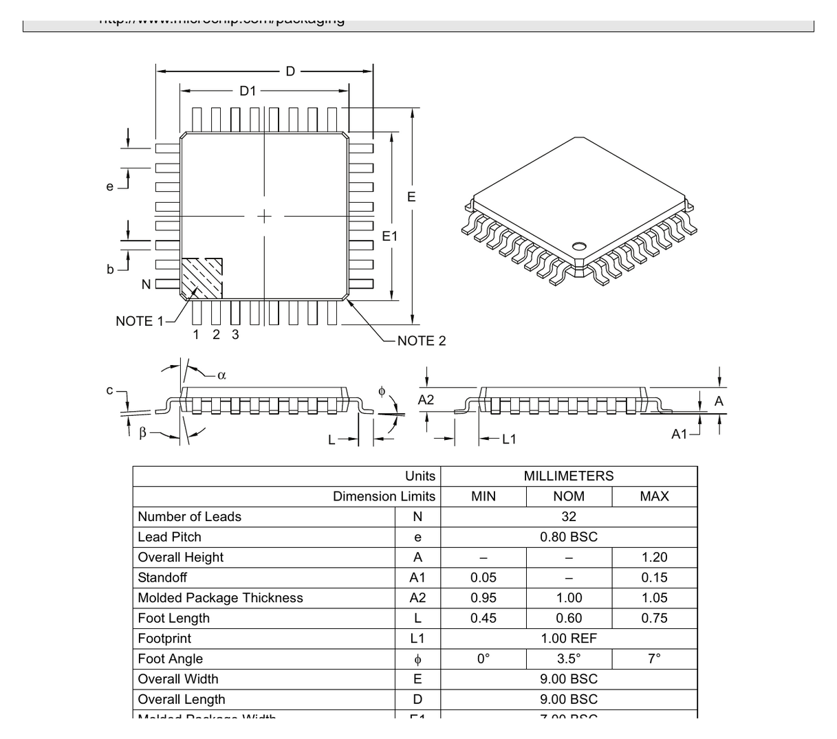
| 32A | 32-lead Thin Quad Flat Pack (TQFP), 1.0 mm body | 7 × 7 × 1.0 mm | 0.80 mm BSC |
| 28M1 | 28-pad Very Thin Quad Flat No-Lead (VQFN) | 4 × 4 × 1.0 mm | 0.45 mm |
| 32M1-A | 32-pad Thin Quad Flat No-Lead (VQFN, S4B) | 5 × 5 × 1.0 mm | 0.50 mm |
Ordering Codes (ATmega328P)
| Code | Package | Temp Range |
|---|---|---|
| ATmega328P-AU / -AUR | 32A (TQFP) | −40 °C to 85 °C |
| ATmega328P-MMH / -MMHR | 28M1 (VQFN) | −40 °C to 85 °C |
| ATmega328P-MU / -MUR | 32M1-A (VQFN) | −40 °C to 85 °C |
| ATmega328P-PU | 28P3 (SPDIP) | −40 °C to 85 °C |
| ATmega328P-AN / -ANR | 32A (TQFP) | −40 °C to 105 °C |
| ATmega328P-MN / -MNR | 32M1-A (VQFN) | −40 °C to 105 °C |
| ATmega328P-PN | 28P3 (SPDIP) | −40 °C to 105 °C |
Suffix R = tape & reel. Suffix N = extended (105 °C) temperature grade. MMH leadframe uses NiPdAu finish.
Applications
- Arduino Uno, Nano, Pro Mini, and compatible development boards
- Hobby and educational microcontroller projects
- Low-power sensor nodes and battery-operated devices (thanks to 0.1 µA power-down)
- Motor control, lighting, and simple industrial automation
- USB-to-serial gadgets, LED controllers, data loggers
- Safety-critical timing with programmable watchdog + brown-out detection
Key Formulas
Speed vs. Supply Voltage
The maximum CPU clock frequency scales linearly with VCC:
$$f_{CLK,,max} = \begin{cases} 4\ \text{MHz} & 1.8\ \text{V} \le V_{CC} \le 2.7\ \text{V} \ 10\ \text{MHz} & 2.7\ \text{V} \le V_{CC} \le 4.5\ \text{V} \ 20\ \text{MHz} & 4.5\ \text{V} \le V_{CC} \le 5.5\ \text{V} \end{cases}$$
I/O Switching Current Estimate
Current drawn on a capacitively-loaded pin is approximately:
$$I_{pin} \approx C_L \cdot V_{CC} \cdot f$$
where $C_L$ is load capacitance, $V_{CC}$ is operating voltage, and $f$ is the average switching frequency of the pin.