AP63357 — 3.8 V to 32 V, 3.5 A Low-IQ Synchronous Buck
UnreviewedDiodes AP63357 (V-DFN3020-13). 3.5 A synchronous buck with 74 mΩ HS + 40 mΩ LS MOSFETs, 22 µA IQ PFM mode, 450 kHz FSS for low EMI, 3.8–32 V input.
Source: Diodes Incorporated AP63356/AP63357 Datasheet
Manufacturer: Diodes Incorporated
Part Number: AP63357 (AP63356/AP63357 family)
Document: DS41949 Rev 3-2, August 2019 (3.8 V to 32 V input, 3.5 A Low-IQ Synchronous Buck with Enhanced EMI Reduction)
Description
The AP63356/AP63357 is a 3.5 A synchronous buck converter with a wide input voltage range of 3.8 V to 32 V. The device fully integrates a 74 mΩ high-side power MOSFET and a 40 mΩ low-side power MOSFET to provide high-efficiency step-down DC-DC conversion.
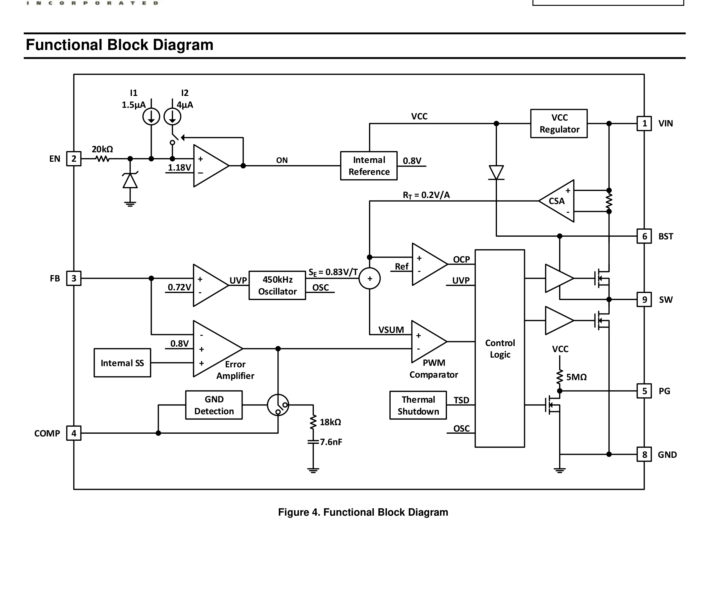
The AP63356/AP63357 device is easily used by minimizing the external component count due to its adoption of peak current mode control along with its integrated loop compensation network.
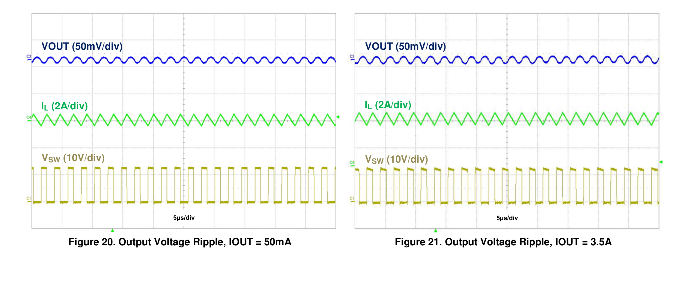
The AP63356/AP63357 design is optimized for Electromagnetic Interference (EMI) reduction. The device has a proprietary gate driver scheme to resist switching node ringing without sacrificing MOSFET turn-on and turn-off times, which reduces high-frequency radiated EMI noise caused by MOSFET switching. The AP63356/AP63357 also features Frequency Spread Spectrum (FSS) with a switching frequency jitter of ±6 %, which reduces EMI by not allowing emitted energy to stay in any one frequency for a significant period of time.
The device is available in a 3 mm × 2 mm V-DFN3020-13 package.
Key Specifications
| Parameter | Value |
|---|---|
| Input Voltage Range | 3.8 V – 32 V |
| Output Current | 3.5 A |
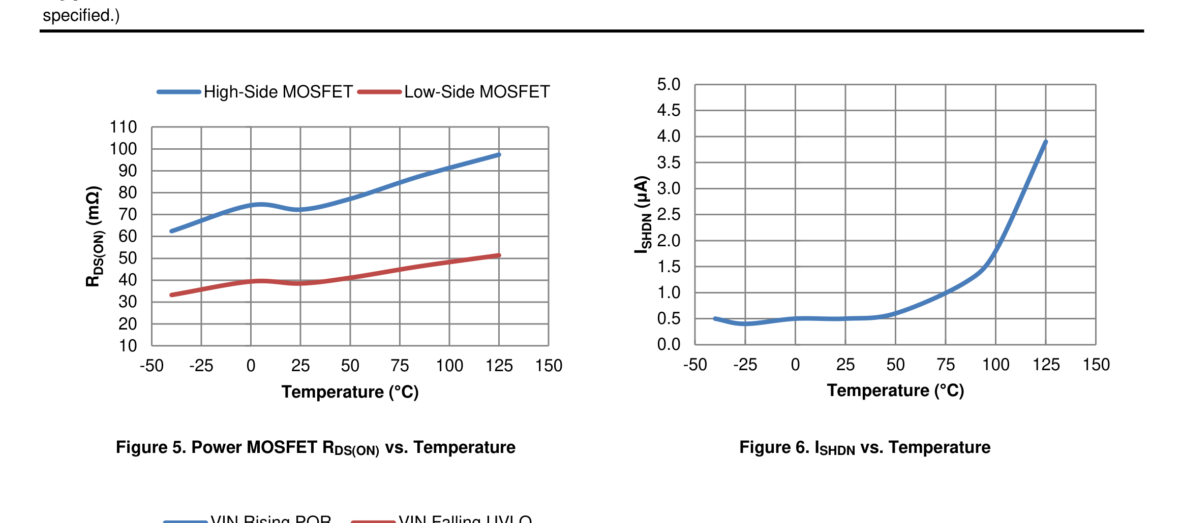
| High-Side MOSFET RDS(on) | 74 mΩ typ |
| Low-Side MOSFET RDS(on) | 40 mΩ typ |
| Reference Voltage Accuracy | 0.8 V ±1 % |
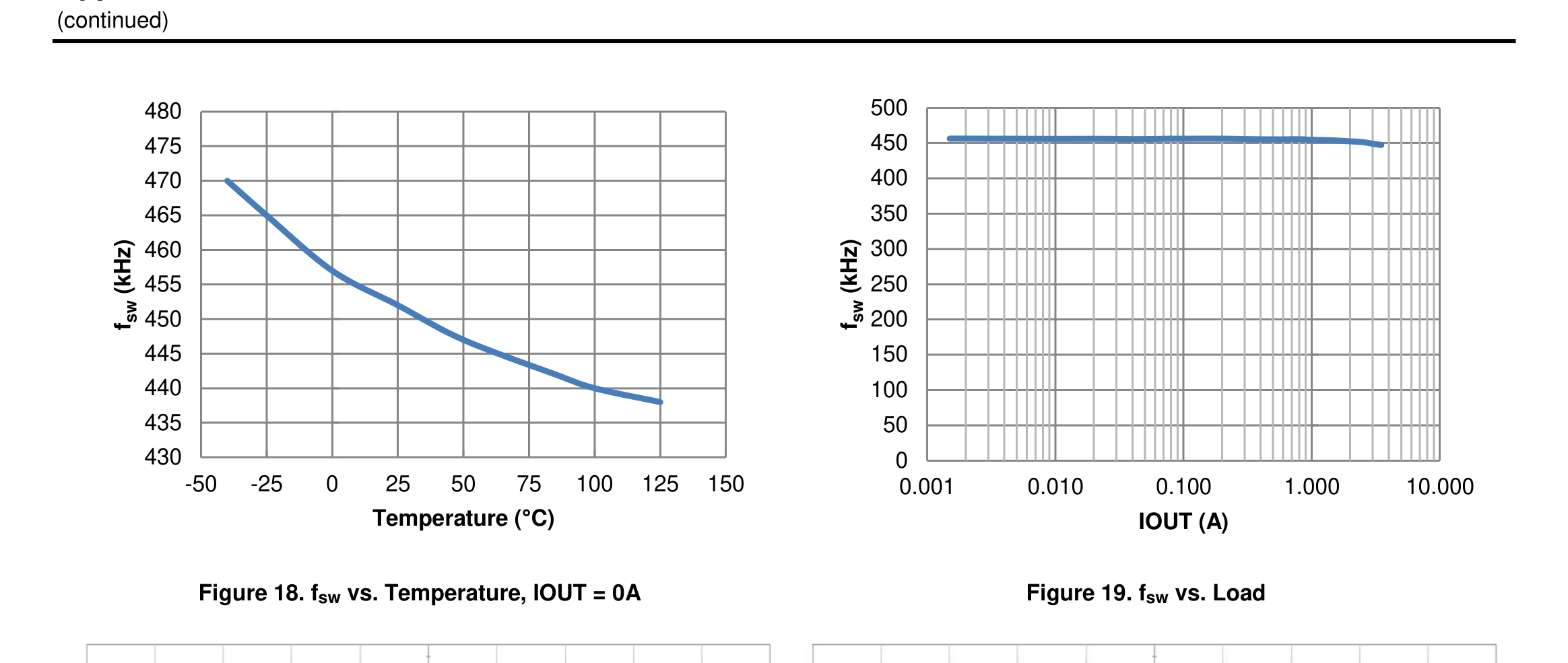
| Switching Frequency | 450 kHz (typ) |
| IQ (Pulse Frequency Modulation) | 22 µA |
| Low-IQ Mode | Yes (AP63357) |
| Frequency Spread Spectrum | ±6 % (FSS) |
| Precision Enable Threshold | 1.18 V (typ) |
| Package | V-DFN3020-13 (3 mm × 2 mm) |
| Operating Temperature | −40 °C to +85 °C (ambient) |
Features
- VIN 3.8 V to 32 V
- 3.5 A continuous output current
- 0.8 V ±1 % reference voltage
- 22 µA low quiescent current (Pulse Frequency Modulation)
- 450 kHz switching
- Pulse Width Modulation (PWM) regardless of output load — AP63356
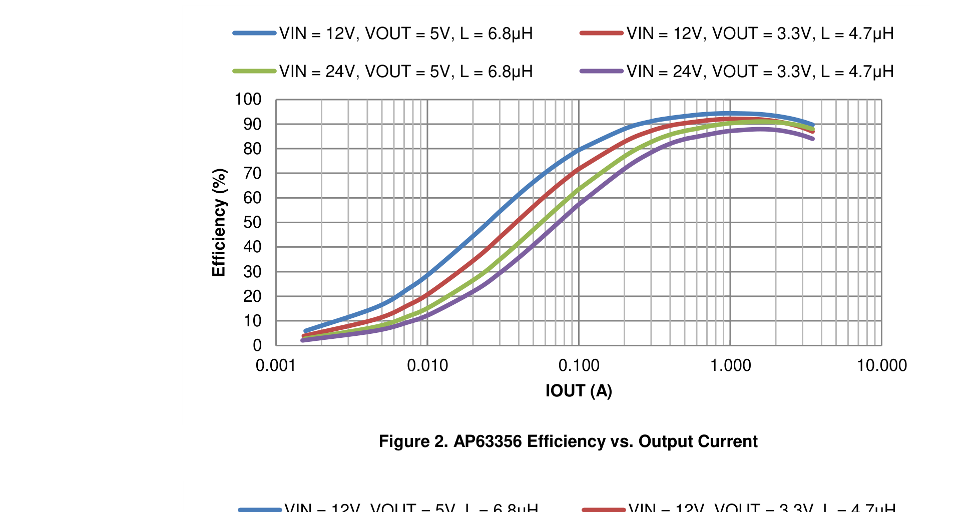
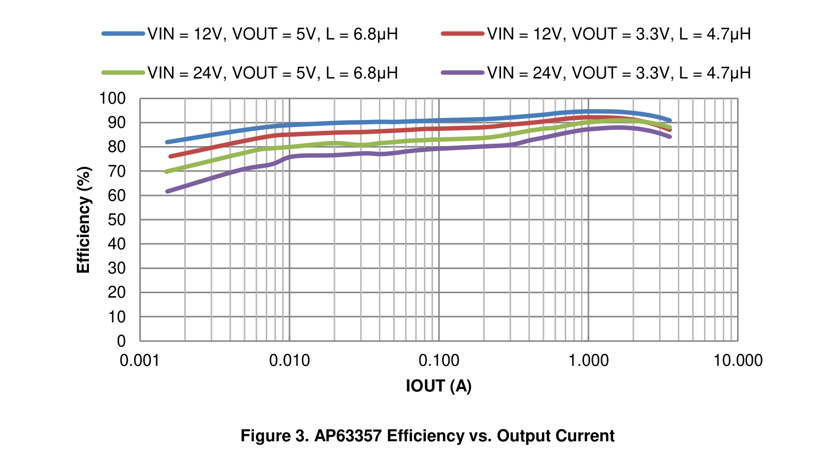
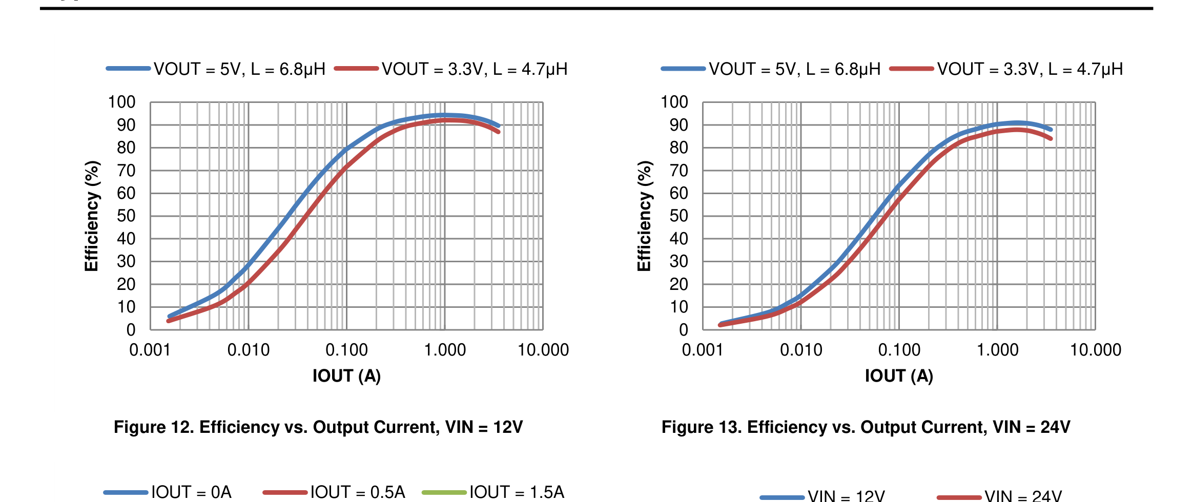
- Supports Pulse Frequency Modulation (PFM) — AP63357 — up to 86 % efficiency at 5 mA light load
- Proprietary gate driver design for best EMI reduction
- Frequency Spread Spectrum (FSS) to reduce EMI
- Low-Dropout (LDO) Mode
- Power Good Indicator with 5 MΩ internal pull-up
- Precision Enable Threshold to Adjust UVLO
- Protection Circuitry:
- Undervoltage lockout (UVLO)
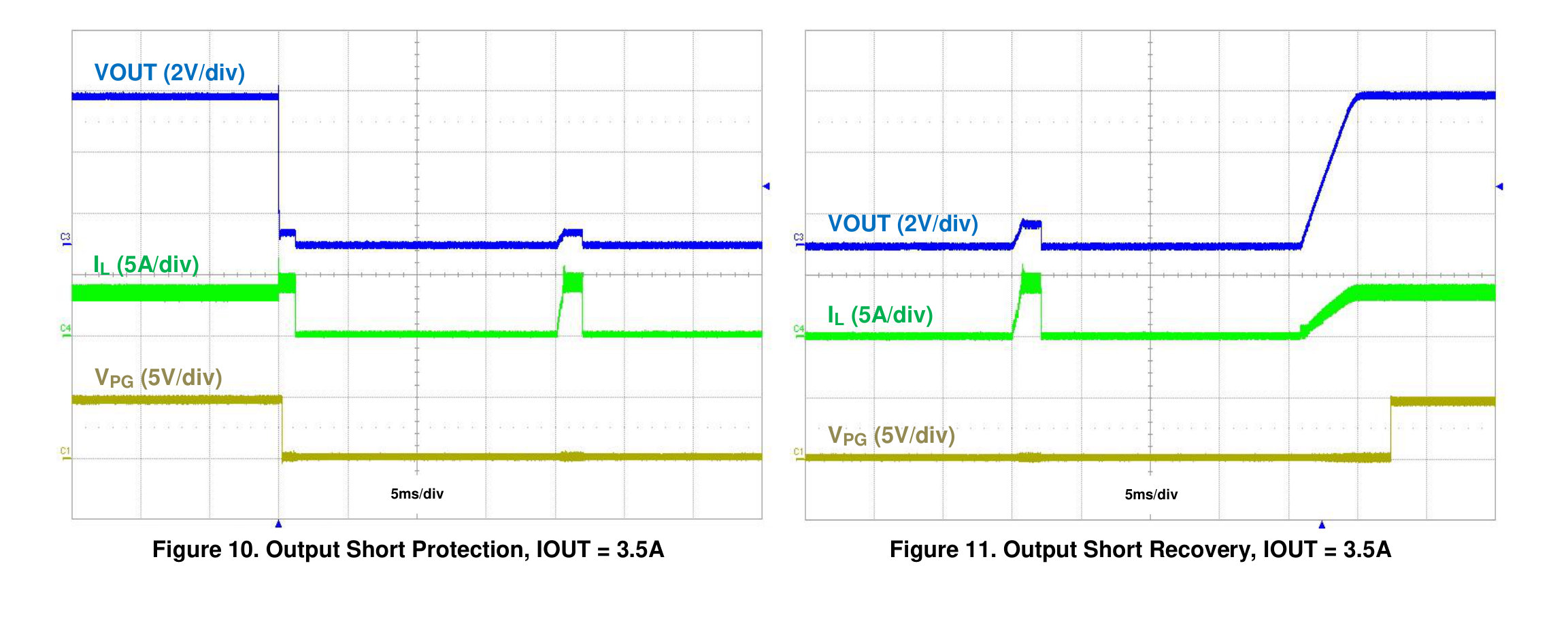
- Output Undervoltage Protection (UVP)
- Cycle-by-cycle peak current limit
- Thermal shutdown
- Totally Lead-Free & Fully RoHS Compliant
- Halogen and Antimony Free — Green Device
Applications
- 5 V, 12 V, and 24 V distributed power bus supplies
- Flat-screen TV sets and monitors
- Power tools and laser printers
- White goods and small home appliances
- FPGA, DSP, and ASIC supplies
- Home audio
- Network systems
- Gaming consoles
- Consumer electronics
- General-purpose point of load
Pin Configuration
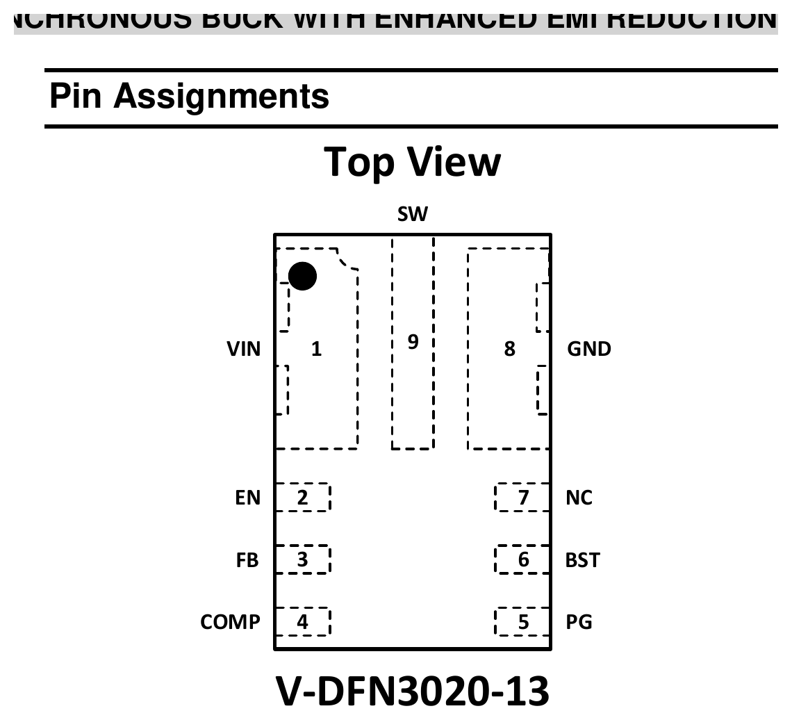
Package: V-DFN3020-13 Top View (Type A).
| Pin | Name | Function |
|---|---|---|
| 1 | VIN | Power Input. Supplies the IC and step-down MOSFETs. Drive VIN with a 3.8 V to 32 V source. Bypass to GND with a suitable large capacitor. |
| 2 | EN | Enable Input. A digital input that turns the regulator on or off. Drive EN high to turn on the regulator and low to turn it off. Connect to VIN or leave floating for automatic startup. Precision threshold of 1.18 V for UVLO programming. |
| 3 | FB | Feedback sensing terminal. Connect this pin to the resistive divider of the output. |
| 4 | COMP | Compensation. Connect the COMP pin to GND to use internal loop compensation. Connect an external RC network to the COMP pin to adjust loop response. |
| 5 | PG | Power Good. Open-drain output with internal 5 MΩ pull-up resistor pulled to GND when the output voltage is out of regulation limits. |
| 6 | BST | High-Side Gate Drive Boost Input. A 100 nF capacitor is recommended from BST to SW to power the high-side driver. |
| 7 | NC | No Connection. |
| 8 | GND | Power Ground. |
| 9 | SW | Power Switching Output. Switching node that supplies power to the output. Connect the output LC filter from SW to the output load. |
Absolute Maximum Ratings
| Symbol | Parameter | Rating | Unit |
|---|---|---|---|
| VIN | Supply Pin Voltage (DC) | −0.3 to +35.0 | V |
| VIN | Supply Pin Voltage (400 ns) | −0.3 to +40.0 | V |
| VEN | Enable/UVLO Pin Voltage | −0.3 to +35.0 | V |
| VFB | Feedback Pin Voltage | −0.3 to +6.0 | V |
| VCOMP | Compensation Pin Voltage | −0.3 to +6.0 | V |
| VPG | Power Good Pin Voltage | −0.3 to +6.0 | V |
| VBST | Bootstrap Pin Voltage | VSW − 0.3 to VSW + 6.0 | V |
| VSW | Switch Pin Voltage (DC) | −0.3 to VIN + 0.3 | V |
| VSW | Switch Pin Voltage (2.5 ns) | −2.5 to VIN + 2.0 | V |
| TST | Storage Temperature | −65 to +150 | °C |
| TJ | Junction Temperature | +170 | °C |
| — | Lead Temperature | +260 | °C |
| ESD (HBM) | Human Body Model | 2000 | V |
| ESD (CDM) | Charged Device Model | 1000 | V |
Thermal Resistance
| Symbol | Parameter | Rating | Unit |
|---|---|---|---|
| θJA | Junction to Ambient, V-DFN3020-13 (Type A) | 25 | °C/W |
| θJC | Junction to Case, V-DFN3020-13 (Type A) | 5 | °C/W |
Recommended Operating Conditions
| Symbol | Parameter | Min | Max | Unit |
|---|---|---|---|---|
| VIN | Supply Voltage | 3.8 | 32 | V |
| VOUT | Output Voltage | 0.8 | 31 | V |
| TA | Operating Ambient Temperature Range | −40 | +85 | °C |
| TJ | Operating Junction Temperature | −40 | +125 | °C |
Electrical Characteristics
TA = +25 °C, VIN = 12 V, unless otherwise specified. Min/Max limits apply across the recommended ambient temperature range −40 °C to +85 °C and input voltage range 3.8 V to 32 V, unless otherwise specified.
| Symbol | Parameter | Test Conditions | Min | Typ | Max | Unit |
|---|---|---|---|---|---|---|
| ISHDN | Shutdown Supply Current | VEN = 0 V | — | 1 | 3 | µA |
| IQ | Quiescent Supply Current (AP63356) | VIN = Floating, VFB = 1.0 V | — | 258 | — | µA |
| IQ | Quiescent Supply Current (AP63357) | VIN = Floating, VFB = 1.0 V | — | 22 | — | µA |
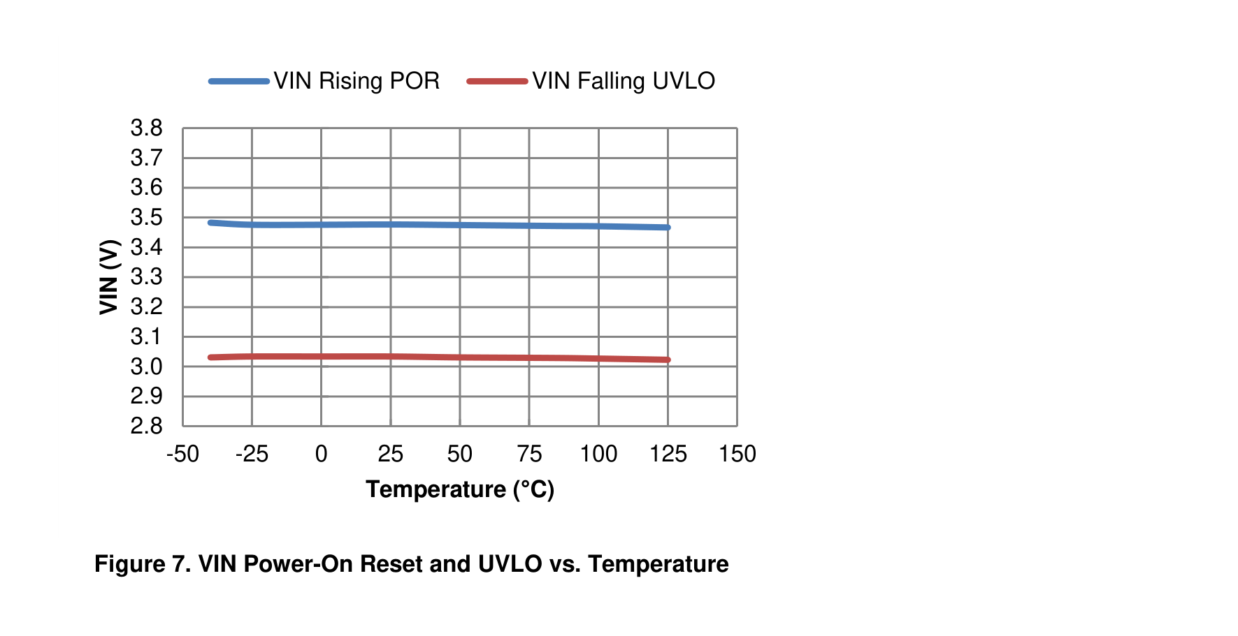
| UVLO | VIN Undervoltage Rising Threshold | — | 3.3 | 3.5 | 3.6 | V |
| UVLO | VIN Undervoltage Hysteresis | — | — | 420 | — | mV |
| RDS(ON)H | High-Side Power MOSFET On-Resistance | — | — | 74 | — | mΩ |
| RDS(ON)L | Low-Side Power MOSFET On-Resistance | — | — | 40 | — | mΩ |
| IPEAK_LIMIT | HS Peak Current Limit | — | 4.0 | 5.0 | 6.0 | A |
| IVALLEY_LIMIT | LS Valley Current Limit | — | 3.2 | 4.2 | 5.2 | A |
| IPFM(PK) | PFM Peak Current Limit | — | — | 700 | — | mA |
| IZC | Zero-Cross Current Threshold | — | — | 0 | — | mA |
| fSW | Oscillator Frequency | — | 400 | 450 | 500 | kHz |
| tON_MIN | Minimum On Time | — | — | 90 | 120 | ns |
| VFB | Feedback Voltage | CCM | 0.792 | 0.800 | 0.808 | V |
| VEN_H | EN Logic High Voltage | — | 1.15 | 1.18 | 1.21 | V |
| VEN_L | EN Logic Low Voltage | — | 1.02 | 1.08 | 1.14 | V |
| IEN | EN Input Current | VEN = 1.5 V | — | 5.5 | — | µA |
| IEN | EN Input Current | VEN = 1 V | — | 1.5 | — | µA |
| tSS | Soft-Start Time | — | — | 4 | — | ms |
| TSD | Thermal Shutdown | — | — | 170 | — | °C |
| THYS | Thermal Shutdown Hysteresis | — | — | 25 | — | °C |
Packages
V-DFN3020-13 (Type A), 3 mm × 2 mm.
Applications
Typical application
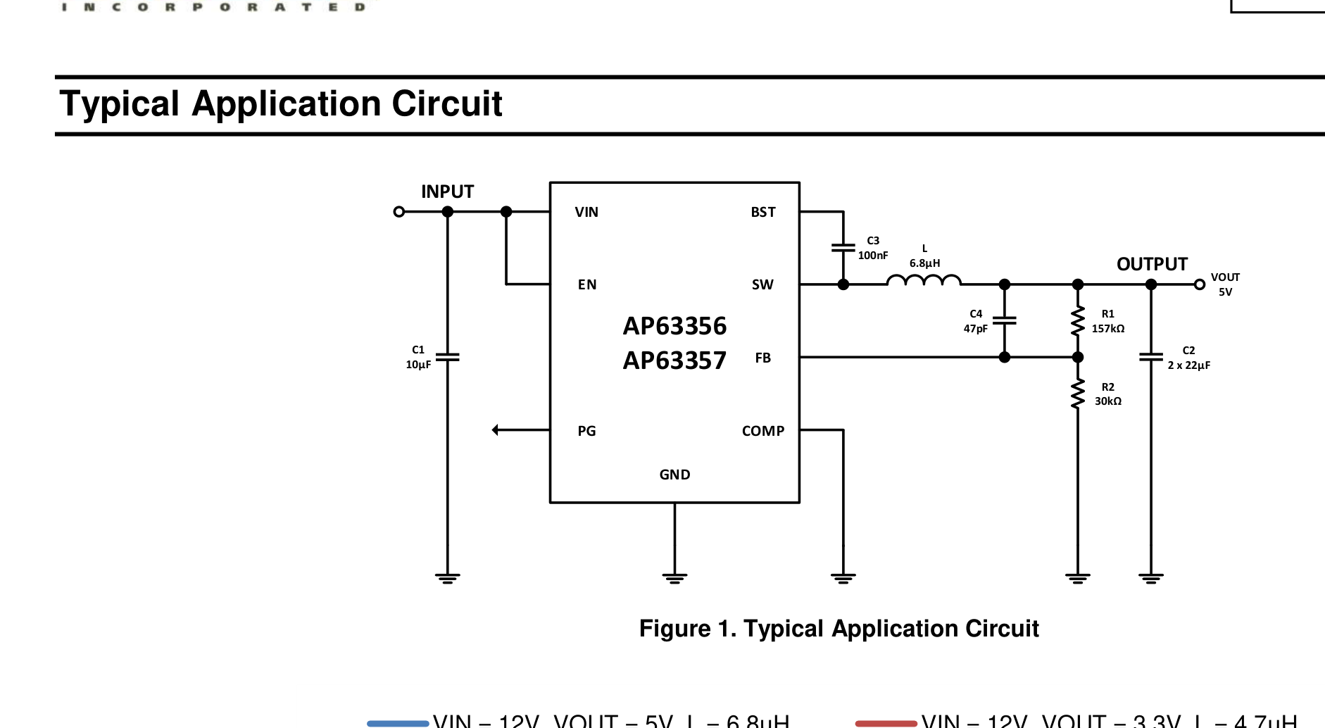
The AP63357 is designed as a standalone synchronous buck with minimal external components. A single 100 nF BST capacitor, input bulk capacitor, output capacitor, inductor, and feedback divider complete a working supply. Optional external RC compensation network via COMP pin is available for loop tuning.
Feedback divider sets output voltage
$$V_{OUT} = 0.8\text{ V} \times \left(1 + \frac{R_{top}}{R_{bot}}\right)$$
EMI control
Frequency Spread Spectrum (FSS) with ±6 % clock jitter reduces EMI without additional components. Proprietary gate driver design controls switch-node slew rate to reduce radiated EMI.