AP2112K — 600 mA CMOS LDO Regulator with Enable
UnreviewedDiodes AP2112. 600 mA CMOS LDO, ±1.5 % accuracy, 2.5–6.0 V input, enable pin, low-quiescent 55 µA, fixed 1.2/1.8/2.5/2.6/3.3 V, SOT25/SOT89-5/SO-8.
Source: Diodes Incorporated AP2112 Datasheet
Manufacturer: Diodes Incorporated
Part Number: AP2112
Document: DS39724 Rev 2-2, June 2017 (600 mA CMOS LDO Regulator with Enable)
Description
The AP2112 is a CMOS process low-dropout linear regulator with enable function. In the regulator version, the regulator delivers a guaranteed 600 mA (min.) continuous load current. The AP2112 is available with a fixed output voltage of 1.2 V, 1.8 V, 2.5 V, 2.6 V, or 3.3 V. The LDO has an output accuracy of ±1.5 % and a very fast loop response providing excellent performance for dealing with line and load transients. The AP2112 includes an auto-discharge function which connects the output to ground via 60 Ω of resistance when the device is disabled.
The regulator features low power consumption and provides SOT25, SOT89-5, and SO-8 packages. Previously SOT-23-5, SOT-89-5, and SOIC-8 packages were respectively identified as SOT23-5, SOT89-5, and SO-8 but have been renamed to match the latest Diodes Incorporated nomenclature.
Key Specifications
| Parameter | Value |
|---|---|
| Output Voltage Accuracy | ±1.5 % |
| Output Current | 600 mA (min) |
| Foldback Short Circuit Protection | 50 mA |
| Enable Function | Active High (ON/OFF VOUT) |
| Low Dropout Voltage (3.3 V) | 250 mV typ @ IOUT = 600 mA |
| Line Regulation | 0.2 % / V (typ) |
| Load Regulation | 0.02 % / mA (typ) |
| Low Quiescent Current | 55 µA (typ) |
| Low Standby Current | 0.01 µA (typ) |
| Low Output Noise | 50 µVRMS |
| PSRR @ 100 Hz | 65 dB |
| PSRR @ 1 kHz | 65 dB |
| ESD (Machine Model) | 400 V |
| ESD (Human Body Model) | 4000 V |
| Operating Temperature | −40 °C to +85 °C |
| Packages | SOT25, SOT89-5, SO-8 |
Features
- Output voltage accuracy ±1.5 %
- Output current 600 mA (min)
- Foldback short-circuit protection 50 mA
- Enable function to turn on/off VOUT
- Low dropout voltage 250 mV (typ) @ 600 mA for 3.3 V version
- Excellent load regulation 0.2 %/A typ
- Excellent line regulation 0.02 %/V typ
- Low quiescent current 55 µA typ
- Low standby current 0.01 µA typ
- Low output noise 50 µVRMS
- PSRR 100 Hz: 65 dB; 1 kHz: 65 dB
- ESD: MM 400 V, HBM 4000 V
- Operating temperature range −40 °C to +85 °C
- Totally lead-free & fully RoHS-compliant
- Halogen and antimony free — "Green" device
Applications
- Laptop computer
- LCD monitor
- Portable DVD
Pin Configuration
Available in SOT25, SOT89-5 (R5/R5A), and SO-8 packages.
| Pin Name | SOT25 | SOT89-5 R5 | SOT89-5 R5A | SO-8 | Function |
|---|---|---|---|---|---|
| VIN | 1 | 4 | 4 | 8 | Input Voltage |
| GND | 2 | 2 | 2 | 6, 7 | GND |
| EN | 3 | 3 | 1 | 5 | Chip Enable. H = normal work, L = shutdown output |
| NC | — | 1 | 3 | 2, 3, 4 | No Connection |
| VOUT | 5 | 5 | 5 | 1 | Output Voltage |
Absolute Maximum Ratings
| Symbol | Parameter | Rating | Unit |
|---|---|---|---|
| VCC | Power Supply Voltage | 6.5 | V |
| TJ | Operating Junction Temperature | +150 | °C |
| TSTG | Storage Temperature | −65 to +150 | °C |
| TLEAD | Lead Temperature (Soldering, 10 s) | +260 | °C |
| θJA (SOT25, no heatsink) | Thermal Resistance | 184 | °C/W |
| θJA (SO-8) | Thermal Resistance | 114 | °C/W |
| θJA (SOT89-5) | Thermal Resistance | 120 | °C/W |
| — | ESD (Machine Model) | 400 | V |
| — | ESD (Human Body Model) | 4000 | V |
Recommended Operating Conditions
| Symbol | Parameter | Min | Max | Unit |
|---|---|---|---|---|
| VIN | Supply Voltage | 2.5 | 6.0 | V |
| TA | Ambient Operation Temperature | −40 | +85 | °C |
Electrical Characteristics
AP2112-1.2 electrical characteristics: @VIN = 2.5 V, CIN = 1.0 µF (ceramic), COUT = 1.0 µF (ceramic), TA = +25 °C, unless otherwise specified.
| Symbol | Parameter | Conditions | Min | Typ | Max | Unit |
|---|---|---|---|---|---|---|
| VOUT | Output Voltage | VIN = 2.5 V, 1 mA ≤ IOUT ≤ 30 mA | VOUT−98.5% | 1.2 | VOUT+101.5% | V |
| IOUT(MAX) | Maximum Output Current | VIN = 2.5 V, VOUT = 1.182 V to 1.218 V | 600 | — | — | mA |
| ΔVOUT/VOUT | Load Regulation | VIN = 2.5 V, 1 mA ≤ IOUT ≤ 600 mA | −1 | 0.2 | 1 | %/A |
| ΔVOUT/VOUT/VIN | Line Regulation | 2.5 V ≤ VIN ≤ 6 V, IOUT = 30 mA | −0.1 | 0.02 | 0.1 | %/V |
| VDROP | Dropout Voltage | IOUT = 10 mA | — | 1000 | 1300 | mV |
| VDROP | Dropout Voltage | IOUT = 300 mA | — | 1000 | 1300 | mV |
| VDROP | Dropout Voltage | IOUT = 600 mA | — | 1000 | 1300 | mV |
| IQ | Quiescent Current | VIN = 2.5 V, IOUT = 0 mA | — | 55 | 80 | µA |
| ISTD | Standby Current | VIN = 2.5 V, VEN in OFF mode | — | 0.01 | 1.0 | µA |
| PSRR | Power Supply Rejection Ratio | Ripple 0.1 VP-P, VIN = 2.5 V, IOUT = 100 mA, f = 100 Hz | — | 65 | — | dB |
| PSRR | Power Supply Rejection Ratio | f = 1 kHz | — | 65 | — | dB |
| ΔVOUT/VOUT/ΔT | Output Voltage Temperature Coefficient | TA = −40 °C to +85 °C | — | ±100 | — | ppm/°C |
| ISHORT | Short Current Limit | VOUT = 0 V | — | 50 | — | mA |
| VNOISE | RMS Output Noise | No Load, 10 Hz ≤ f ≤ 100 kHz | — | 50 | — | µVRMS |
| VH | VEN High Voltage | Enable logic high, regulator on | 1.5 | — | 6.0 | V |
| VL | VEN Low Voltage | Enable logic low, regulator off | 0 | — | 0.4 | V |
| — | Start-up Time | No Load | — | 20 | — | µs |
| RPD | EN Pull-Down Resistor | — | — | 3.0 | — | MΩ |
| RDCHG | VOUT Discharge Resistor | Set EN pin at Low | — | 60 | — | Ω |
| TOTSD | Thermal Shutdown Temperature | — | — | +160 | — | °C |
| THYSTSD | Thermal Shutdown Hysteresis | — | — | ±25 | — | °C |
Applications
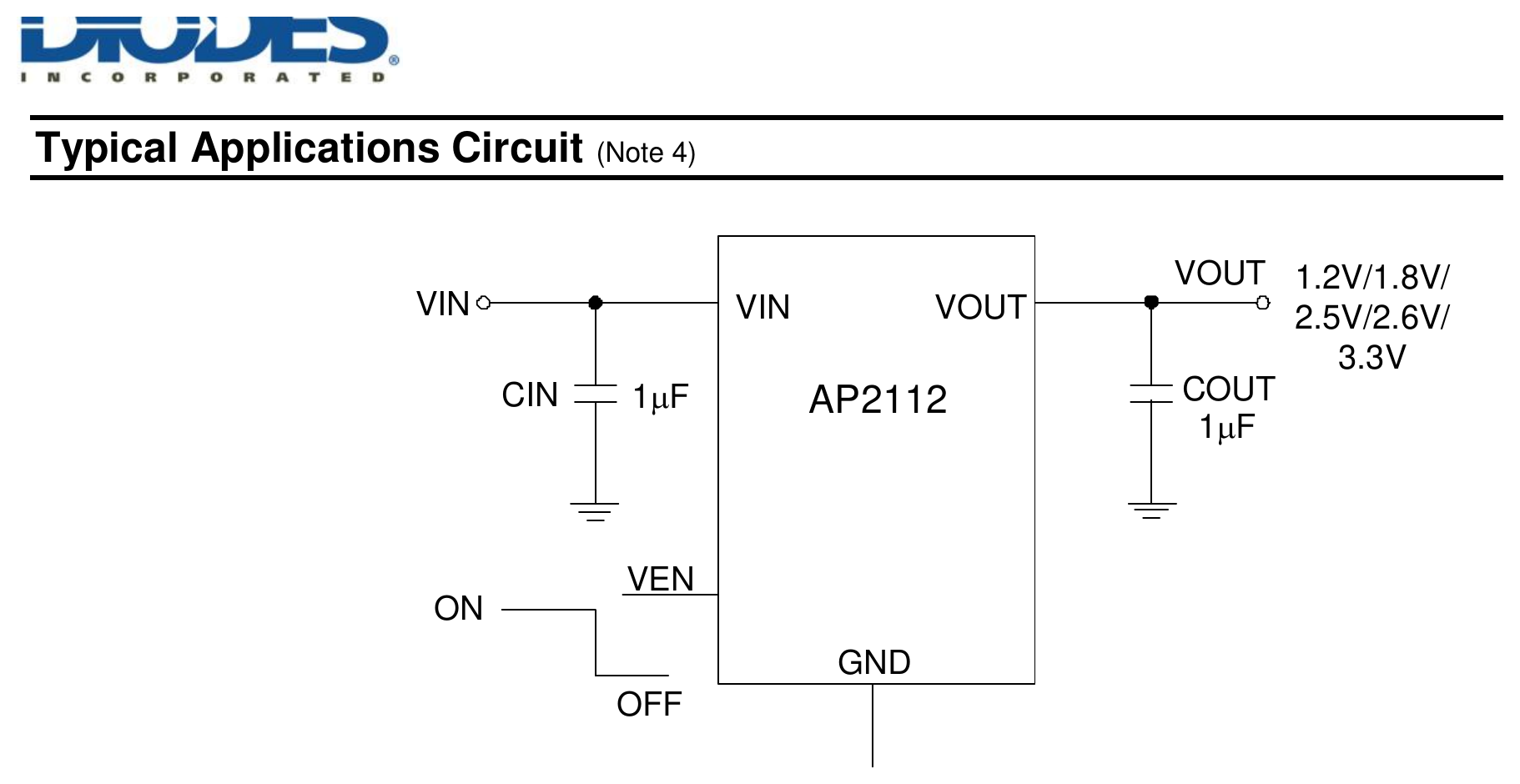
Typical Application Circuit
VIN feeds through a 1 µF ceramic capacitor CIN to the VIN pin. The VEN pin switches the regulator on (H) and off (L). VOUT connects through a 1 µF ceramic capacitor COUT (X7R or X5R dielectric recommended if 1.0 µF ceramic capacitor is selected as input/output capacitors).
Key Formulas
Short-circuit behavior — the foldback current limit kicks in at roughly:
$$I_{SHORT} \approx 50\text{ mA}$$
while normal operation allows IOUT up to 600 mA. Quiescent current scales with temperature with a coefficient of ±100 ppm/°C.