AOZ1282CI — 1.2 A Simple Buck Regulator
UnreviewedAlpha & Omega Semiconductor AOZ1282CI EZBuck. 4.5–36 V input, 1.2 A output adjustable down to 0.8 V, 450 kHz PWM, internal 420 mΩ NMOS, SOT23-6L.
Source: Alpha & Omega AOZ1282CI Datasheet
Manufacturer: Alpha & Omega Semiconductor
Part Number: AOZ1282CI
Document: Rev 1.4 — June 2022 (EZBuck™ 1.2 A Simple Buck Regulator)
Description
The AOZ1282CI is a high-efficiency, simple-to-use 1.2 A buck regulator flexible enough to be optimized for a variety of applications. The AOZ1282CI works from a 4.5 V to 36 V input voltage range and provides up to 1.2 A of continuous output current. The output voltage is adjustable down to 0.8 V. The fixed switching frequency of 450 kHz PWM operation reduces inductor size.
Key Specifications
| Parameter | Value |
|---|---|
| Input Voltage Range | 4.5 V – 36 V |
| Output Current | 1.2 A continuous |
| Output Voltage | Adjustable down to 0.8 V |
| Switching Frequency | 450 kHz (fixed PWM) |
| Internal NMOS RDS(on) | 420 mΩ |
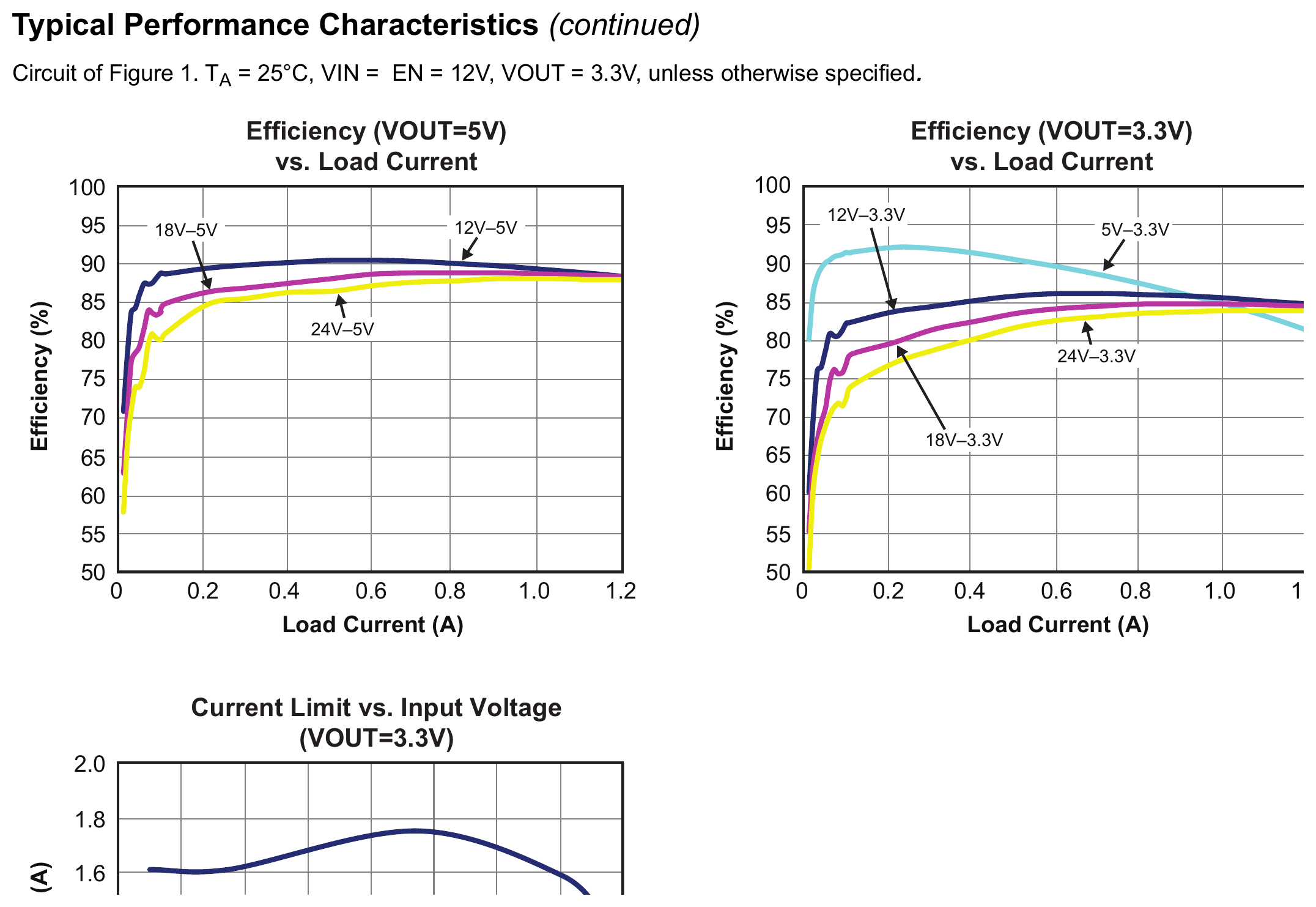
| Efficiency | Up to 95 % |
| Package | SOT23-6L |
| Operating Temperature | −40 °C to +85 °C (ambient) |
Features
- 4.5 V to 36 V operating input voltage range
- 420 mΩ internal NMOS
- Up to 95 % efficiency
- Internal compensation
- 1.2 A continuous output current
- Fixed 450 kHz PWM operation
- Internal soft start
- Output voltage adjustable down to 0.8 V
- Cycle-by-cycle current limit
- Short-circuit protection
- Thermal shutdown
- Small-size SOT23-6L package
Applications
- Telecom / Networking / Datacom equipment
- Point-of-load DC/DC conversion
- Set-top boxes and cable modems
- DVD drives and HDDs
- LCD monitors and TVs
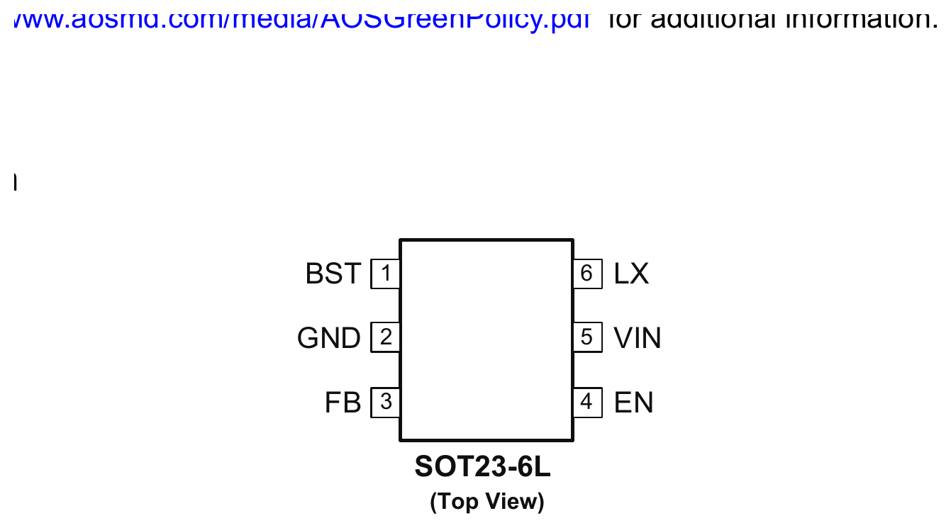
Pin Configuration
Package: SOT23-6L (Top View).
| Pin | Name | Function |
|---|---|---|
| 1 | BST | Bootstrap Voltage Input. High-side driver supply. Connect a 100 nF capacitor between BST and LX. |
| 2 | GND | Ground |
| 3 | FB | Feedback Input. Regulated to 0.8 V. Used to set the PWM output voltage via a resistor divider between the output and GND. |
| 4 | EN | Enable Pin. Active high. Connect EN pin to VIN through a current-limiting resistor. Do not leave EN floating. |
| 5 | VIN | Supply Voltage Input. 4.5 V to 36 V. When VIN rises above the UVLO threshold, the device starts up. |
| 6 | LX | PWM Output. Connect to inductor. |
Absolute Maximum Ratings
Exceeding the Absolute Maximum Ratings may damage the device.
| Parameter | Rating | Units |
|---|---|---|
| Supply Voltage (VIN) | 40 | V |
| LX to GND | −0.7 to VIN+0.3 | V |
| LX to GND transient, < 10 ns | −3 | V |
| EN to GND | −0.3 to 40 | V |
| FB to GND | −0.3 to 6 | V |
| BST to GND | VLX + 6 | V |
| Junction Temperature (TJ) | +150 | °C |
| Storage Temperature (TS) | −65 to +150 | °C |
| ESD Rating (HBM, 1.5 kΩ + 100 pF) | 2 | kV |
Recommended Operating Conditions
| Parameter | Rating |
|---|---|
| Supply Voltage (VIN) | 4.5 V to 36 V |
| Output Voltage (VOUT) | 0.8 V to 0.85×VIN |
| Ambient Temperature (TA) | −40 °C to +85 °C |
| Package Thermal Resistance (θJA) | 220 °C/W (SOT23-6L) |
Electrical Characteristics
TA = 25 °C, VIN = 12 V, unless otherwise specified. Bold indicates temperature range of −40 °C to +85 °C.
| Parameter | Symbol | Conditions | Min | Typ | Max | Units |
|---|---|---|---|---|---|---|
| Supply Voltage | VIN | 4.5 | 36 | V | ||
| Input Under-Voltage Lockout Threshold | VUVLO | VIN rising / falling | 2.3 | 2.9 | V | |
| UVLO Hysteresis | VUVLO_HYS | 260 | mV | |||
| Quiescent Supply Current | IIN | IOUT = 0, FB = 1 V, EN > 1.2 V | 1 | 1.5 | mA | |
| Shutdown Supply Current | IOFF | EN = 0 V | 8 | µA | ||
| Feedback Voltage | VFB | 784 | 800 | 816 | mV | |
| Load Regulation | VFB_LOAD | 0.12 A < Load < 1.08 A | 0.5 | % | ||
| Line Regulation | VFB_LINE | Load = 600 mA | 0.03 | %/V | ||
| FB Input Current | IFB | FB = Regulation | 500 | nA | ||
| EN Input Threshold (Off) | VEN_OFF | Off threshold | 0.4 | V | ||
| EN Input Threshold (On) | VEN_ON | On threshold | 1.2 | V | ||
| EN Input Hysteresis | VEN_HYS | 200 | mV | |||
| EN Input Current | IEN | 3 | µA | |||
| Switching Frequency | fO | 360 | 450 | 540 | kHz | |
| Maximum Duty Cycle | DMAX | 87 | % | |||
| Minimum On Time | tON_MIN | 150 | ns | |||
| Current Limit | ILIM | 1.5 | 1.9 | A | ||
| Thermal Shutdown Limit (TJ rising) | TSD | 150 | °C | |||
| Thermal Shutdown Limit (TJ falling) | 110 | °C | ||||
| Soft-Start Interval | tSS | 1.5 | ms | |||
| NMOS Leakage | ILEAKAGE | EN = 0, LX = 0 | 10 | µA | ||
| NMOS On-Resistance | RDS(on) | 420 | mΩ |
Key Formulas
Feedback divider sets output voltage:
$$V_{OUT} = 0.8\text{ V} \times \left(1 + \frac{R_1}{R_2}\right)$$
Output capacitor ripple (low-ESR ceramic):
$$\Delta V_{OUT} \approx \frac{\Delta I_L}{8 \times f \times C_O}$$
Total power dissipation (conduction-loss dominated):
$$P_{total_loss} = (V_{IN} \times I_{IN}) - (V_{OUT} \times V_{IN})$$
Applications
- Typical application: the Figure 1 reference circuit uses an external inductor L, output capacitor C2, bootstrap capacitor C3, and feedback resistors R1/R2. Enable pin should be driven by VIN through a current-limiting resistor.
- Output-capacitor selection: use ceramic (X5R/X7R) capacitors for low ESR and tight ripple; low-ESR tantalum or aluminum electrolytic also work.
- Layout: the two high-current loops — input path VIN→C₁→switch and output path LX→L→COUT→Schottky — should both be kept tight to minimize noise and improve efficiency.