AMS1117 — 1A Low Dropout Voltage Regulator
UnreviewedThe AMS1117 is a 1A low-dropout linear voltage regulator from Advanced Monolithic Systems, available in adjustable and fixed (1.5V, 1.8V, 2.5V, 2.85V, 3.3V, 5.0V) versions in SOT-223, TO-252, and SO-8
Source: Advanced Monolithic Systems Datasheet
Manufacturer: Advanced Monolithic Systems, Inc.
Part Number: AMS1117
Document: AMS1117 Datasheet (undated)
Description
The AMS1117 series of adjustable and fixed voltage regulators are designed to provide up to 1A output current and to operate down to 1V input-to-output differential. The dropout voltage of the device is guaranteed at a maximum of 1.3V, decreasing at lower load currents.
On-chip trimming adjusts the reference voltage to 1.5%. Current limit is set to minimize the stress under overload conditions on both the regulator and power source circuitry.
The AMS1117 devices are pin compatible with other three-terminal SCSI regulators and are offered in the low profile surface mount SOT-223 package, in the 8L SOIC package and in the TO-252 (DPAK) plastic package.
Key Specifications
| Parameter | Value |
|---|---|
| Output Current | 1A |
| Dropout Voltage | 1.1V typ, 1.3V max |
| Input Voltage | Up to 15V |
| Fixed Output Options | 1.5V, 1.8V, 2.5V, 2.85V, 3.3V, 5.0V |
| Line Regulation | 0.2% max |
| Load Regulation | 0.4% max |
| Operating Junction Temp | -40°C to 125°C |
| Storage Temperature | -65°C to +150°C |
| Packages | SOT-223, TO-252, SO-8 |
| Pin Count | 3 (SOT-223, TO-252), 8 (SOIC) |
| RoHS Compliant | Yes |
Features
- Three terminal adjustable or fixed voltages: 1.5V, 1.8V, 2.5V, 2.85V, 3.3V and 5.0V
- Output current of 1A
- Operates down to 1V dropout
- Line regulation: 0.2% max
- Load regulation: 0.4% max
- SOT-223, TO-252 and SO-8 package available
Pin Configuration
3-Pin Fixed/Adjustable Version (SOT-223, TO-252)
| Pin | Name | Description |
|---|---|---|
| 1 | GND/ADJ | Ground (fixed versions) or Adjust (adjustable version) |
| 2 | V_OUT | Regulated output voltage |
| 3 | V_IN | Input voltage |
8-Pin SOIC Version
| Pin | Name | Description |
|---|---|---|
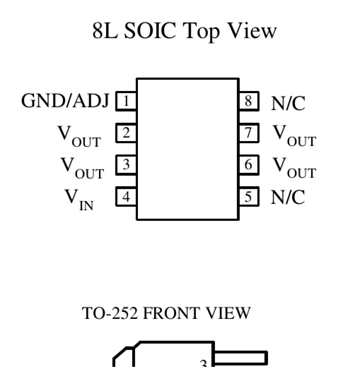
| 1 | GND/ADJ | Ground (fixed) or Adjust (adjustable) |
| 2 | V_OUT | Regulated output voltage |
| 3 | V_OUT | Regulated output voltage |
| 4 | V_IN | Input voltage |
| 5 | N/C | No connection |
| 6 | V_OUT | Regulated output voltage |
| 7 | V_OUT | Regulated output voltage |
| 8 | N/C | No connection |
Absolute Maximum Ratings
| Parameter | Value |
|---|---|
| Power Dissipation | Internally limited |
| Input Voltage | 15V |
| Operating Junction Temperature (Control Section) | -40°C to 125°C |
| Operating Junction Temperature (Power Transistor) | -40°C to 125°C |
| Storage Temperature | -65°C to +150°C |
| Lead Temperature (25 sec soldering) | 265°C |
Thermal Resistance
| Package | θ_JA |
|---|---|
| SO-8 | 160°C/W |
| TO-252 | 80°C/W |
| SOT-223 | 90°C/W* |
*With package soldering to copper area over backside ground plane or internal power plane, θ_JA can vary from 46°C/W to >90°C/W depending on mounting technique and the size of the copper area.
Recommended Operating Conditions
| Parameter | Min | Max | Unit |
|---|---|---|---|
| Input Voltage | V_OUT + 1.0 | 15 | V |
| Output Current | 10 mA (min load) | 1.0 | A |
Electrical Characteristics
Electrical Characteristics at I_OUT = 0 mA, and T_J = +25°C unless otherwise specified. Parameters identified with boldface type apply over the full operating temperature range.
Reference Voltage
| Parameter | Device | Conditions | Min | Typ | Max | Unit |
|---|---|---|---|---|---|---|
| Reference Voltage | AMS1117 | I_OUT = 10 mA, 1.5V ≤ (V_IN - V_OUT) ≤ 12V | 1.232 | 1.250 | 1.268 | V |
| Reference Voltage (full temp) | AMS1117 | I_OUT = 10 mA, 1.5V ≤ (V_IN - V_OUT) ≤ 12V | 1.2125 | 1.250 | 1.2875 | V |
Output Voltage (Fixed Versions)
| Device | Conditions | Min | Typ | Max | Unit |
|---|---|---|---|---|---|
| AMS1117-1.5 | V_IN = 3V | 1.478 / 1.455 | 1.500 / 1.500 | 1.522 / 1.545 | V |
| AMS1117-1.8 | V_IN = 3.3V | 1.773 / 1.746 | 1.800 / 1.800 | 1.827 / 1.854 | V |
| AMS1117-2.5 | V_IN = 4V | 2.463 / 2.425 | 2.500 / 2.500 | 2.537 / 2.575 | V |
| AMS1117-2.85 | V_IN = 4.35V | 2.808 / 2.7645 | 2.850 / 2.850 | 2.892 / 2.9355 | V |
| AMS1117-3.3 | V_IN = 4.8V | 3.251 / 3.201 | 3.300 / 3.300 | 3.349 / 3.399 | V |
| AMS1117-5.0 | V_IN = 6.5V | 4.925 / 4.850 | 5.000 / 5.000 | 5.075 / 5.150 | V |
Line Regulation
| Device | Conditions | Typ | Max | Unit |
|---|---|---|---|---|
| AMS1117 (adj) | 1.5V ≤ (V_IN - V_OUT) ≤ 12V | 0.015 / 0.035 | 0.2 / 0.2 | % |
| AMS1117-1.5 | 1.5V ≤ (V_IN - V_OUT) ≤ 12V | 0.3 / 0.6 | 5 / 6 | mV |
| AMS1117-1.8 | 1.5V ≤ (V_IN - V_OUT) ≤ 12V | 0.3 / 0.6 | 5 / 6 | mV |
| AMS1117-2.5 | 1.5V ≤ (V_IN - V_OUT) ≤ 12V | 0.3 / 0.6 | 6 / 6 | mV |
| AMS1117-2.85 | 1.5V ≤ (V_IN - V_OUT) ≤ 12V | 0.3 / 0.6 | 6 / 6 | mV |
| AMS1117-3.3 | 1.5V ≤ (V_IN - V_OUT) ≤ 12V | 0.5 / 1.0 | 10 / 10 | mV |
| AMS1117-5.0 | 1.5V ≤ (V_IN - V_OUT) ≤ 12V | 0.5 / 1.0 | 10 / 10 | mV |
Load Regulation
| Device | Conditions | Typ | Max | Unit |
|---|---|---|---|---|
| AMS1117 (adj) | (V_IN - V_OUT) = 1.5V, 10mA ≤ I_OUT ≤ 0.8A | 0.1 / 0.2 | 0.3 / 0.4 | % |
| AMS1117-1.5 | V_IN = 3V, 0 ≤ I_OUT ≤ 0.8A | 3 / 6 | 10 / 20 | mV |
| AMS1117-1.8 | V_IN = 3.3V, 0 ≤ I_OUT ≤ 0.8A | 3 / 6 | 10 / 20 | mV |
| AMS1117-2.5 | V_IN = 5V, 0 ≤ I_OUT ≤ 0.8A | 3 / 6 | 12 / 20 | mV |
| AMS1117-2.85 | V_IN = 4.35V, 0 ≤ I_OUT ≤ 0.8A | 3 / 6 | 12 / 20 | mV |
| AMS1117-3.3 | V_IN = 4.75V, 0 ≤ I_OUT ≤ 0.8A | 3 / 7 | 15 / 25 | mV |
| AMS1117-5.0 | V_IN = 6.5V, 0 ≤ I_OUT ≤ 0.8A | 5 / 10 | 20 / 35 | mV |
Other Electrical Parameters
| Parameter | Device | Conditions | Min | Typ | Max | Unit |
|---|---|---|---|---|---|---|
| Dropout Voltage | AMS1117-1.5/-1.8/-2.5/-2.85/-3.3/-5.0 | ΔV_OUT, ΔV_REF = 1%, I_OUT = 0.8A (Note 4) | — | 1.1 | 1.3 | V |
| Current Limit | AMS1117-1.5/-1.8/-2.5/-2.85/-3.3/-5.0 | (V_IN - V_OUT) = 1.5V | 900 | 1,100 | 1,500 | mA |
| Minimum Load Current | AMS1117 | (V_IN - V_OUT) = 1.5V (Note 5) | — | 5 | 10 | mA |
| Quiescent Current | AMS1117-1.5/-1.8/-2.5/-2.85/-3.3/-5.0 | (V_IN - V_OUT) = 1.5V | — | 5 | 11 | mA |
| Ripple Rejection | AMS1117 | f=120Hz, C_OUT=22µF Tantalum, I_OUT=1A, (V_IN-V_OUT)≥3V, C_ADJ=10µF | 60 | 75 | — | dB |
| Ripple Rejection | AMS1117-1.5/-1.8/-2.5/-2.85 | f=120Hz, C_OUT=22µF Tantalum, I_OUT=1A, V_IN=4.35V | 60 | 72 | — | dB |
| Ripple Rejection | AMS1117-3.3 | f=120Hz, C_OUT=22µF Tantalum, I_OUT=1A, V_IN=4.75V | 60 | 72 | — | dB |
| Ripple Rejection | AMS1117-5.0 | f=120Hz, C_OUT=22µF Tantalum, I_OUT=1A, V_IN=6.5V | 60 | 68 | — | dB |
| Thermal Regulation | AMS1117 | T_A=25°C, 30ms pulse | — | 0.008 | 0.04 | %/W |
| Adjust Pin Current | AMS1117 | I_OUT=10mA, 1.5V≤(V_IN-V_OUT)≤12V | — | 55 | 120 | µA |
| Adjust Pin Current Change | AMS1117 | I_OUT=10mA, 1.5V≤(V_IN-V_OUT)≤12V | — | 0.2 | 5 | µA |
| Temperature Stability | — | — | — | 0.5 | — | % |
| Long Term Stability | — | T_A=125°C, 1000Hrs | — | 0.3 | 1 | % |
| RMS Output Noise (% of V_OUT) | — | T_A=25°C, 10Hz ≤ f ≤ 10kHz | — | 0.003 | — | % |
| Thermal Resistance Junction-to-Case | — | All packages | — | — | 15 | °C/W |
Notes
Note 1: Absolute Maximum Ratings indicate limits beyond which damage to the device may occur. For guaranteed specifications and test conditions, see the Electrical Characteristics. The guaranteed specifications apply only for the test conditions listed.
Note 2: Line and Load regulation are guaranteed up to the maximum power dissipation of 1.2 W for SOT-223, 2.2W for TO-252 and 780mW for 8-Lead SOIC. Power dissipation is determined by the input/output differential and the output current. Guaranteed maximum power dissipation will not be available over the full input/output range.
Note 3: See thermal regulation specifications for changes in output voltage due to heating effects. Line and load regulation are measured at a constant junction temperature by low duty cycle pulse testing. Load regulation is measured at the output lead ~1/8" from the package.
Note 4: Dropout voltage is specified up to 0.8A load. For currents over 0.8A dropout will be higher.
Note 5: Minimum load current is defined as the minimum output current required to maintain regulation. When 1.5V ≤ (V_IN - V_OUT) ≤ 12V the device is guaranteed to regulate if the output current is greater than 10mA.
Thermal Information
Copper Area vs. Thermal Resistance (Table 1)
| Top Side (Sq. mm) | Back Side (Sq. mm) | Board Area (Sq. mm) | θ_JA (Junction-to-Ambient) |
|---|---|---|---|
| 2500 | 2500 | 2500 | 55°C/W |
| 1000 | 2500 | 2500 | 55°C/W |
| 225 | 2500 | 2500 | 65°C/W |
| 100 | 2500 | 2500 | 80°C/W |
| 1000 | 1000 | 1000 | 60°C/W |
| 1000 | 0 | 1000 | 65°C/W |
Tab of device attached to topside copper. Data taken using 1/16" FR-4 board with 1 oz. copper foil.
The thermal resistance from the junction to the tab for the AMS1117 is 15°C/W. Thermal resistance from tab to ambient can be as low as 30°C/W. The total thermal resistance from junction to ambient can be as low as 45°C/W.
The power dissipation of the AMS1117 is equal to:
$$P_D = (V_{IN} - V_{OUT}) \times I_{OUT}$$
Maximum junction temperature will be equal to:
$$T_J = T_{A(MAX)} + P_D \times \theta_{JA}$$
Maximum junction temperature must not exceed 125°C.
Ripple Rejection Design Notes
The ripple rejection values are measured with the adjustment pin bypassed. The impedance of the adjust pin capacitor at the ripple frequency should be less than the value of R1 (normally 100Ω to 200Ω) for a proper bypassing and ripple rejection approaching the values shown. The size of the required adjust pin capacitor is a function of the input ripple frequency. If R1=100Ω at 120Hz the adjust pin capacitor should be >13µF. At 10kHz only 0.16µF is needed.
The ripple rejection will be a function of output voltage, in circuits without an adjust pin bypass capacitor. The output ripple will increase directly as a ratio of the output voltage to the reference voltage (V_OUT / V_REF).
Applications
- High efficiency linear regulators
- Post regulators for switching supplies
- 5V to 3.3V linear regulator
- Battery chargers
- Active SCSI terminators
- Power management for notebooks
- Battery powered instrumentation
Application Hints
The AMS1117 series of adjustable and fixed regulators are easy to use and are protected against short circuit and thermal overloads. Thermal protection circuitry will shut-down the regulator should the junction temperature exceed 165°C at the sense point. Pin compatible with older three terminal adjustable regulators, these devices offer the advantage of a lower dropout voltage, more precise reference tolerance and improved reference stability with temperature.
Stability
The circuit design used in the AMS1117 series requires the use of an output capacitor as part of the device frequency compensation. The addition of 22µF solid tantalum on the output will ensure stability for all operating conditions. When the adjustment terminal is bypassed with a capacitor to improve the ripple rejection, the requirement for an output capacitor increases. The value of 22µF tantalum covers all cases of bypassing the adjustment terminal. Without bypassing the adjustment terminal smaller capacitors can be used with equally good results.
To further improve stability and transient response of these devices larger values of output capacitor can be used.
Protection Diodes
Unlike older regulators, the AMS1117 family does not need any protection diodes between the adjustment pin and the output and from the output to the input to prevent over-stressing the die. Internal resistors are limiting the internal current paths on the AMS1117 adjustment pin, therefore even with capacitors on the adjustment pin no protection diode is needed to ensure device safety under short-circuit conditions.
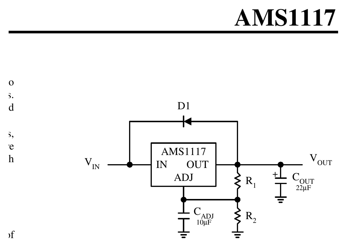
Diodes between the input and output are not usually needed. Microsecond surge currents of 50A to 100A can be handled by the internal diode between the input and output pins of the device. In normal operations it is difficult to get those values of surge currents even with the use of large output capacitances. If high value output capacitors are used, such as 1000µF to 5000µF and the input pin is instantaneously shorted to ground, damage can occur. A diode from output to input is recommended, when a crowbar circuit at the input of the AMS1117 is used (Figure 1).
Output Voltage (Adjustable Version)
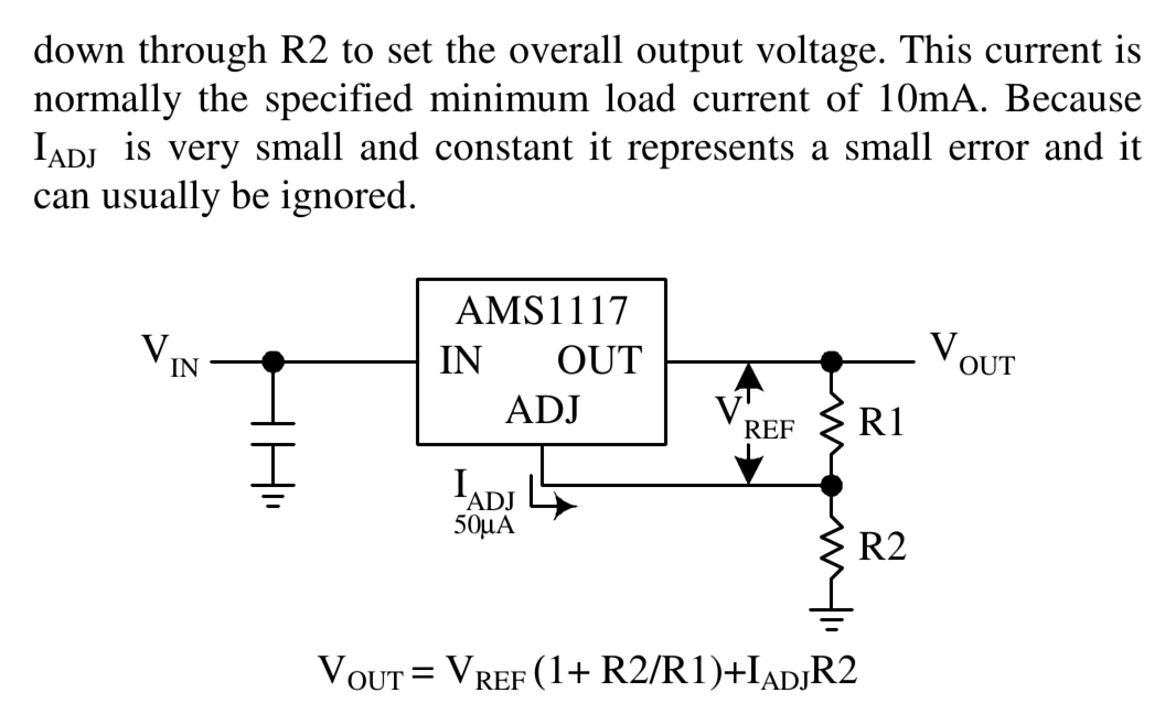
The AMS1117 series develops a 1.25V reference voltage between the output and the adjust terminal. Placing a resistor between these two terminals causes a constant current to flow through R1 and down through R2 to set the overall output voltage. This current is normally the specified minimum load current of 10mA. Because I_ADJ is very small and constant it represents a small error and it can usually be ignored.
See Figure 2 — Basic Adjustable Regulator (uploaded as screenshot asset)
Key Formulas
Adjustable Output Voltage
$$V_{OUT} = V_{REF} \times \left(1 + \frac{R2}{R1}\right) + I_{ADJ} \times R2$$
Effective Resistance with Parasitic Line Resistance
$$R_{eff} = \frac{R_P \times (R2 + R1)}{R1}$$
where $R_P$ = Parasitic Line Resistance
Power Dissipation
$$P_D = (V_{IN} - V_{OUT}) \times I_{OUT}$$
Maximum Junction Temperature
$$T_J = T_{A(MAX)} + P_D \times \theta_{JA}$$
Packages
Ordering Information
| Part Number | Package | Part Number | Package |
|---|---|---|---|
| AMS1117CD | TO-252 | AMS1117 | SOT-223 |
| AMS1117CD-1.5 | TO-252 | AMS1117-1.5 | SOT-223 |
| AMS1117CD-1.8 | TO-252 | AMS1117-1.8 | SOT-223 |
| AMS1117CD-2.5 | TO-252 | AMS1117-2.5 | SOT-223 |
| AMS1117CD-2.85 | TO-252 | AMS1117-2.85 | SOT-223 |
| AMS1117CD-3.3 | TO-252 | AMS1117-3.3 | SOT-223 |
| AMS1117CD-5.0 | TO-252 | AMS1117-5.0 | SOT-223 |
| AMS1117CS | SO-8 | AMS1117CS-1.5 | SO-8 |
| AMS1117CS-1.8 | SO-8 | AMS1117CS-2.5 | SO-8 |
| AMS1117CS-2.85 | SO-8 | AMS1117CS-3.3 | SO-8 |
| AMS1117CS-5.0 | SO-8 | — | — |
Temperature Range
All parts: -40°C to 125°C operating junction temperature.
TO-252 Plastic Package (D)
See package drawing (uploaded as screenshot asset — pkg-to252.png)
Dimensions (inches, millimeters in parentheses):
- Body width: 0.255–0.265 (6.48–6.73)
- Body length: 0.380–0.410 (9.65–10.41)
- Lead width: 0.025 (0.635) TYP
- Lead pitch: 0.156–0.204 (3.96–5.18)
- Tab width: 0.206–0.214 (5.23–5.44)
- Tab length: 0.235–0.245 (5.969–6.223)
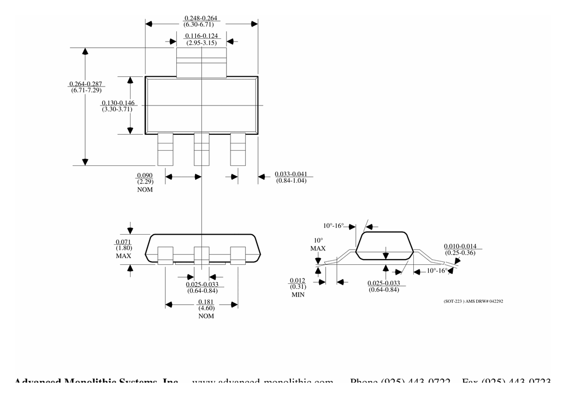
3 Lead SOT-223 Plastic Package
See package drawing (uploaded as screenshot asset — pkg-sot223.png)
Dimensions (inches, millimeters in parentheses):
- Body width: 0.248–0.264 (6.30–6.71)
- Body length: 0.264–0.287 (6.71–7.29)
- Lead width: 0.033–0.041 (0.84–1.04)
- Tab width: 0.116–0.124 (2.95–3.15)
- Lead pitch: 0.090 (2.29) NOM
- Overall height: 0.071 (1.80) MAX
8 Lead SOIC Plastic Package (S)
See package drawing (uploaded as screenshot asset — pkg-soic8.png)
Dimensions (inches, millimeters in parentheses):
- Body width: 0.189–0.197* (4.801–5.004)
- Body length: 0.228–0.244 (5.791–6.197)
- Lead width: 0.014–0.019 (0.355–0.483)
- Lead pitch: 0.050 (1.270) TYP
- Overall height: 0.053–0.069 (1.346–1.752)
- Molded body width: 0.150–0.157** (3.810–3.988)
*Dimension does not include mold flash. Mold flash shall not exceed 0.006" (0.152mm) per side.
**Dimension does not include interlead flash. Interlead flash shall not exceed 0.010" (0.254mm) per side.
Typical Performance Characteristics
Six characteristic curves are provided:
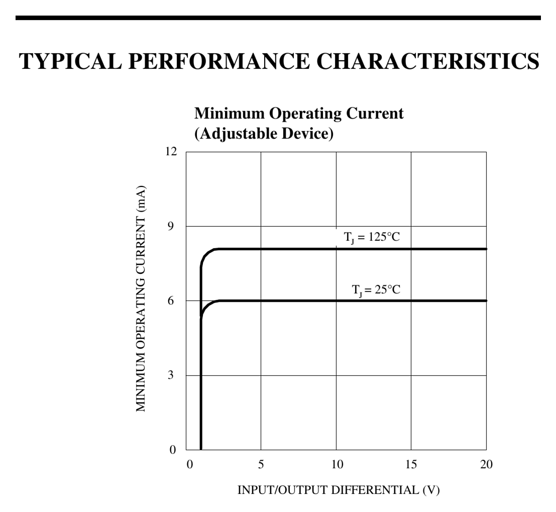
Minimum Operating Current (Adjustable Device) — Shows minimum operating current (mA) vs. input/output differential (V) at T_J = 25°C and T_J = 125°C. Current is ~5mA at 5V differential, rising to ~10mA at 15V.
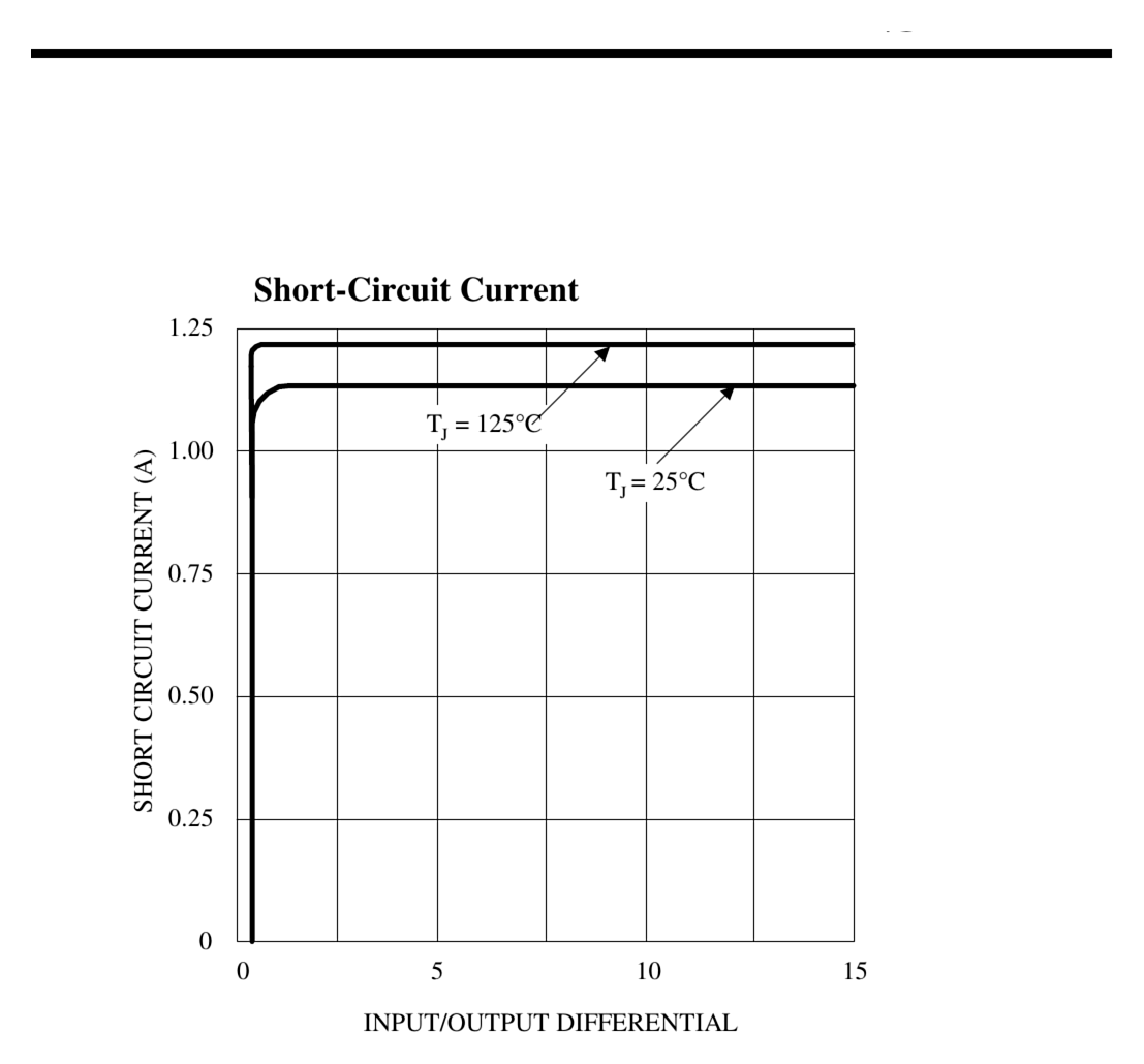
Short-Circuit Current — Shows short-circuit current (A) vs. input/output differential at T_J = 25°C and T_J = 125°C. At 25°C, current peaks at ~1.1A near 5V differential.
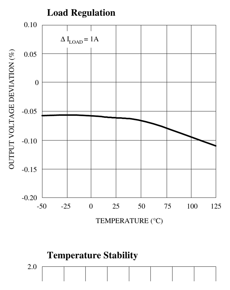
Load Regulation — Shows output voltage deviation (%) vs. temperature (°C) at ΔI_LOAD = 1A. Deviation stays within ±0.05% across -50°C to 125°C.
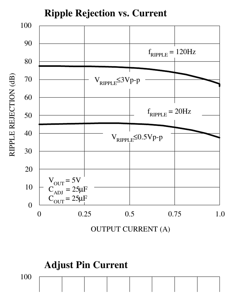
Ripple Rejection vs. Current — Shows ripple rejection (dB) vs. output current (A). At f_RIPPLE = 120Hz with V_RIPPLE ≤ 3Vp-p: ~77dB at low current, dropping to ~67dB at 1A. At f_RIPPLE = 20Hz with V_RIPPLE ≤ 0.5Vp-p: ~45dB across the range.
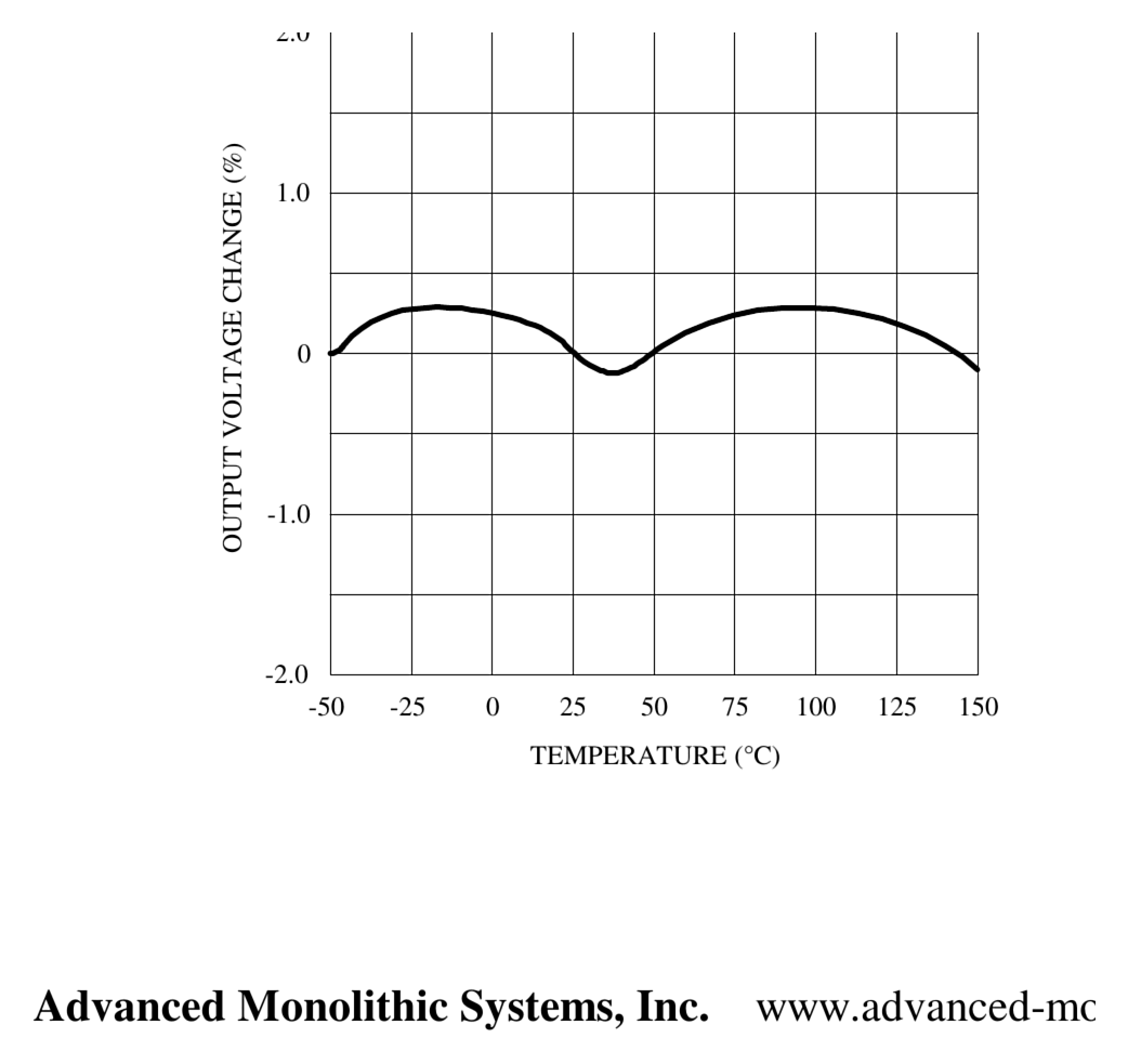
Temperature Stability — Shows output voltage change (%) vs. temperature (°C). Change stays within ±1% from -50°C to 150°C.
Adjust Pin Current — Shows adjust pin current (µA) vs. temperature (°C). Current is ~55µA at 25°C, relatively stable across temperature range.
See all curves (uploaded as screenshot assets)
Load Regulation Design Notes
True remote load sensing is not possible to provide, because the AMS1117 is a three terminal device. The resistance of the wire connecting the regulator to the load will limit the load regulation. The data sheet specification for load regulation is measured at the bottom of the package. Negative side sensing is a true Kelvin connection, with the bottom of the output divider returned to the negative side of the load.
The best load regulation is obtained when the top of the resistor divider R1 is connected directly to the case not to the load. If R1 were connected to the load, the effective resistance between the regulator and the load would be:
$$R_{eff} = \frac{R_P \times (R2 + R1)}{R1}$$
See Figure 3 — Connections for Best Load Regulation (uploaded as screenshot asset)
In the case of fixed voltage devices the top of R1 is connected Kelvin internally, and the ground pin can be used for negative side sensing.
Thermal Considerations
The AMS1117 series have internal power and thermal limiting circuitry designed to protect the device under overload conditions. However maximum junction temperature ratings of 125°C should not be exceeded under continuous normal load conditions. Careful consideration must be given to all sources of thermal resistance from junction to ambient. For the surface mount package SOT-223 additional heat sources mounted near the device must be considered. The heat dissipation capability of the PC board and its copper traces is used as a heat sink for the device.