STM32F103C8T6

STMicroelectronicsActive

Arm Cortex-M3 32-bit MCU, 72 MHz, 64 KB Flash, 20 KB SRAM. USB, CAN, seven timers, two ADCs, nine communication interfaces. The workhorse Blue Pill microcontroller.

Package LQFP-48Body 7 x 7 x 1.4 mmPitch 0.5 mm Pins 48Core Cortex-M3
An interactive library view is below: schematic symbol, PCB footprint (with layer toggles), and the datasheet pin map, all cross-linked. The platform's native 3D / symbol / footprint viewers are at the top of the page; downloadable CAD and the datasheet PDF are on the Files tab (.kicad_sym, .kicad_mod, .step, .glb).

Library view hover any pin, pad, or row — symbol, footprint, and pin map light up together with the datasheet function

POWER (9)

PinNameTypeFunction (datasheet)
1VBATPowerBackup battery supply for RTC and backup registers. Typical operating range 1.8 to 3.6 V. Supplies the RTC and backup domain when VDD is off.
8VSSAPowerAnalog ground reference for ADC, reset block, PLL, and analog peripherals. Connect to digital ground at a single point.
9VDDAPowerAnalog supply for ADC, reset block, PLL, and analog I/O. 2.0 to 3.6 V. Decouple with 1 µF + 10 nF close to the pin.
23VSS_1PowerDigital ground, group 1. Connect to the ground plane; keep short return path to VDD_1 decoupling.
24VDD_1PowerDigital supply, group 1. 2.0 to 3.6 V. Decouple with 100 nF close to the pin.
35VSS_2PowerDigital ground, group 2. Connect to the ground plane; pair with VDD_2 decoupling.
36VDD_2PowerDigital supply, group 2. 2.0 to 3.6 V. Decouple with 100 nF close to the pin.
47VSS_3PowerDigital ground, group 3. Connect to the ground plane; pair with VDD_3 decoupling.
48VDD_3PowerDigital supply, group 3. 2.0 to 3.6 V. Decouple with 100 nF close to the pin.

GPIO (26)

PinNameTypeFunction (datasheet)
2PC13-TAMPER-RTCI/OGPIO port C bit 13, muxed with TAMPER input and RTC output. Supplied through the backup power switch (limited to 3 mA sink); output speed limited to 2 MHz with max 30 pF load; must not source current.
10PA0-WKUPI/OGPIO port A bit 0, 5 V-tolerant when configured as digital input. Alternate functions: standby WKUP, USART2_CTS (remap), ADC12_IN0, TIM2_CH1_ETR.
11PA1I/OGPIO port A bit 1. Alternate functions: USART2_RTS, ADC12_IN1, TIM2_CH2.
12PA2I/OGPIO port A bit 2. Alternate functions: USART2_TX, ADC12_IN2, TIM2_CH3.
13PA3I/OGPIO port A bit 3. Alternate functions: USART2_RX, ADC12_IN3, TIM2_CH4.
14PA4I/OGPIO port A bit 4. Alternate functions: SPI1_NSS, USART2_CK, ADC12_IN4.
15PA5I/OGPIO port A bit 5. Alternate functions: SPI1_SCK, ADC12_IN5.
16PA6I/OGPIO port A bit 6. Alternate functions: SPI1_MISO, ADC12_IN6, TIM3_CH1; remap: TIM1_BKIN.
17PA7I/OGPIO port A bit 7. Alternate functions: SPI1_MOSI, ADC12_IN7, TIM3_CH2; remap: TIM1_CH1N.
18PB0I/OGPIO port B bit 0. Alternate functions: ADC12_IN8, TIM3_CH3; remap: TIM1_CH2N.
19PB1I/OGPIO port B bit 1. Alternate functions: ADC12_IN9, TIM3_CH4; remap: TIM1_CH3N.
20PB2I/OGPIO port B bit 2, 5 V-tolerant. Doubles as BOOT1 boot mode selection input sampled at reset.
21PB10I/OGPIO port B bit 10, 5 V-tolerant. Alternate functions: I2C2_SCL, USART3_TX; remap: TIM2_CH3.
22PB11I/OGPIO port B bit 11, 5 V-tolerant. Alternate functions: I2C2_SDA, USART3_RX; remap: TIM2_CH4.
25PB12I/OGPIO port B bit 12, 5 V-tolerant. Alternate functions: SPI2_NSS, I2C2_SMBAl, USART3_CK, TIM1_BKIN.
26PB13I/OGPIO port B bit 13, 5 V-tolerant. Alternate functions: SPI2_SCK, USART3_CTS, TIM1_CH1N.
27PB14I/OGPIO port B bit 14, 5 V-tolerant. Alternate functions: SPI2_MISO, USART3_RTS, TIM1_CH2N.
28PB15I/OGPIO port B bit 15, 5 V-tolerant. Alternate functions: SPI2_MOSI, TIM1_CH3N.
29PA8I/OGPIO port A bit 8, 5 V-tolerant. Alternate functions: USART1_CK, TIM1_CH1, MCO (master clock output).
30PA9I/OGPIO port A bit 9, 5 V-tolerant. Alternate functions: USART1_TX, TIM1_CH2.
31PA10I/OGPIO port A bit 10, 5 V-tolerant. Alternate functions: USART1_RX, TIM1_CH3.
41PB5I/OGPIO port B bit 5 (NOT 5 V-tolerant on this pin). Alternate functions: I2C1_SMBAl; remap: TIM3_CH2, SPI1_MOSI.
42PB6I/OGPIO port B bit 6, 5 V-tolerant. Alternate functions: I2C1_SCL, TIM4_CH1; remap: USART1_TX.
43PB7I/OGPIO port B bit 7, 5 V-tolerant. Alternate functions: I2C1_SDA, TIM4_CH2; remap: USART1_RX.
45PB8I/OGPIO port B bit 8, 5 V-tolerant. Alternate functions: TIM4_CH3; remap: I2C1_SCL, CANRX.
46PB9I/OGPIO port B bit 9, 5 V-tolerant. Alternate functions: TIM4_CH4; remap: I2C1_SDA, CANTX.

TIMING (4)

PinNameTypeFunction (datasheet)
3PC14-OSC32_INI/OGPIO port C bit 14, muxed with 32 kHz LSE oscillator input (OSC32_IN). Backup-domain pin routed through the power switch; same 2 MHz / 30 pF drive limitation as PC13.
4PC15-OSC32_OUTI/OGPIO port C bit 15, muxed with 32 kHz LSE oscillator output (OSC32_OUT). Backup-domain pin routed through the power switch; same 2 MHz / 30 pF drive limitation as PC13/PC14.
5PD0-OSC_INI/OHSE crystal oscillator input (OSC_IN) after reset; remappable to GPIO PD0 by software. In GPIO mode limited to 50 MHz output. Connect to 4-16 MHz crystal or external clock.
6PD1-OSC_OUTI/OHSE crystal oscillator output (OSC_OUT) after reset; remappable to GPIO PD1 by software. In GPIO mode limited to 50 MHz output.

CONTROL (2)

PinNameTypeFunction (datasheet)
7NRSTI/OActive-low bidirectional device reset. Pulled low by internal or external reset sources; external pull-up recommended (typ 40 kΩ internal weak pull-up).
44BOOT0Boot mode selection input sampled at reset (with BOOT1/PB2): selects boot from Flash, System memory (bootloader), or embedded SRAM. Must be tied to a defined logic level.

USB (2)

PinNameTypeFunction (datasheet)
32PA11I/OGPIO port A bit 11, 5 V-tolerant. Alternate functions: USART1_CTS, CANRX, USBDM (USB D-), TIM1_CH4.
33PA12I/OGPIO port A bit 12, 5 V-tolerant. Alternate functions: USART1_RTS, CANTX, USBDP (USB D+), TIM1_ETR.

DEBUG (5)

PinNameTypeFunction (datasheet)
34PA13I/OGPIO port A bit 13, 5 V-tolerant. Default after reset: JTMS/SWDIO (serial-wire debug data/JTAG mode select). Can be released to GPIO via SWJ-DP disable.
37PA14I/OGPIO port A bit 14, 5 V-tolerant. Default after reset: JTCK/SWCLK (serial-wire debug clock/JTAG clock).
38PA15I/OGPIO port A bit 15, 5 V-tolerant. Default after reset: JTDI (JTAG data in). Remappable to TIM2_CH1_ETR/PA15/SPI1_NSS.
39PB3I/OGPIO port B bit 3, 5 V-tolerant. Default after reset: JTDO / TRACESWO. Remappable to TIM2_CH2, PB3, SPI1_SCK.
40PB4I/OGPIO port B bit 4, 5 V-tolerant. Default after reset: NJTRST (JTAG reset, active low). Remappable to TIM3_CH1, PB4, SPI1_MISO.

Datasheet key pages the pages worth looking at first · pick a page, click it to go full screen

Featuresdatasheet p.1
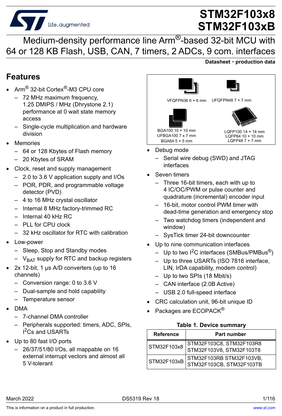
Features

Specifications microcontroller

CoreARM Cortex-M3 CATALOG
Max frequency72 MHz CATALOG
Flash64 KB CATALOG
RAM20 KB CATALOG
GPIO37 CATALOG
Supply (min)2 V CATALOG
Supply (max)3.6 V CATALOG

Peripherals

TIM x4 (16-bit)ADC x2 (12-bit)USARTSPII2CCANUSB 2.0 FS

Provenance

Pin functions extracted by ds2sf from the ST datasheet (116 pages, sha256 0596dd57693c, source lcsc); Claude cites pages and refuses to fabricate, flagging muxed pins for review. CAD from KiCad official libraries (CC-BY-SA 4.0). Footprint pads carry KiCad pinfunction/pintype. 3D board-context composed with cadquery (FR4 + copper pads + solder + pin 1) and rendered via step2glb. Datasheet: ST STM32F103x8/xB.