STM32F103C8T6
STMicroelectronicsActiveArm Cortex-M3 32-bit MCU, 72 MHz, 64 KB Flash, 20 KB SRAM. USB, CAN, seven timers, two ADCs, nine communication interfaces. The workhorse Blue Pill microcontroller.
An interactive library view is below: schematic symbol, PCB footprint (with layer toggles), and the datasheet pin map, all cross-linked. The platform's native 3D / symbol / footprint viewers are at the top of the page; downloadable CAD and the datasheet PDF are on the Files tab (
.kicad_sym, .kicad_mod, .step, .glb).Library view hover any pin, pad, or row — symbol, footprint, and pin map light up together with the datasheet function
POWER (9)
| Pin | Name | Type | Function (datasheet) |
|---|---|---|---|
| 1 | VBAT | Power | Backup battery supply for RTC and backup registers. Typical operating range 1.8 to 3.6 V. Supplies the RTC and backup domain when VDD is off. |
| 8 | VSSA | Power | Analog ground reference for ADC, reset block, PLL, and analog peripherals. Connect to digital ground at a single point. |
| 9 | VDDA | Power | Analog supply for ADC, reset block, PLL, and analog I/O. 2.0 to 3.6 V. Decouple with 1 µF + 10 nF close to the pin. |
| 23 | VSS_1 | Power | Digital ground, group 1. Connect to the ground plane; keep short return path to VDD_1 decoupling. |
| 24 | VDD_1 | Power | Digital supply, group 1. 2.0 to 3.6 V. Decouple with 100 nF close to the pin. |
| 35 | VSS_2 | Power | Digital ground, group 2. Connect to the ground plane; pair with VDD_2 decoupling. |
| 36 | VDD_2 | Power | Digital supply, group 2. 2.0 to 3.6 V. Decouple with 100 nF close to the pin. |
| 47 | VSS_3 | Power | Digital ground, group 3. Connect to the ground plane; pair with VDD_3 decoupling. |
| 48 | VDD_3 | Power | Digital supply, group 3. 2.0 to 3.6 V. Decouple with 100 nF close to the pin. |
GPIO (26)
| Pin | Name | Type | Function (datasheet) |
|---|---|---|---|
| 2 | PC13-TAMPER-RTC | I/O | GPIO port C bit 13, muxed with TAMPER input and RTC output. Supplied through the backup power switch (limited to 3 mA sink); output speed limited to 2 MHz with max 30 pF load; must not source current. |
| 10 | PA0-WKUP | I/O | GPIO port A bit 0, 5 V-tolerant when configured as digital input. Alternate functions: standby WKUP, USART2_CTS (remap), ADC12_IN0, TIM2_CH1_ETR. |
| 11 | PA1 | I/O | GPIO port A bit 1. Alternate functions: USART2_RTS, ADC12_IN1, TIM2_CH2. |
| 12 | PA2 | I/O | GPIO port A bit 2. Alternate functions: USART2_TX, ADC12_IN2, TIM2_CH3. |
| 13 | PA3 | I/O | GPIO port A bit 3. Alternate functions: USART2_RX, ADC12_IN3, TIM2_CH4. |
| 14 | PA4 | I/O | GPIO port A bit 4. Alternate functions: SPI1_NSS, USART2_CK, ADC12_IN4. |
| 15 | PA5 | I/O | GPIO port A bit 5. Alternate functions: SPI1_SCK, ADC12_IN5. |
| 16 | PA6 | I/O | GPIO port A bit 6. Alternate functions: SPI1_MISO, ADC12_IN6, TIM3_CH1; remap: TIM1_BKIN. |
| 17 | PA7 | I/O | GPIO port A bit 7. Alternate functions: SPI1_MOSI, ADC12_IN7, TIM3_CH2; remap: TIM1_CH1N. |
| 18 | PB0 | I/O | GPIO port B bit 0. Alternate functions: ADC12_IN8, TIM3_CH3; remap: TIM1_CH2N. |
| 19 | PB1 | I/O | GPIO port B bit 1. Alternate functions: ADC12_IN9, TIM3_CH4; remap: TIM1_CH3N. |
| 20 | PB2 | I/O | GPIO port B bit 2, 5 V-tolerant. Doubles as BOOT1 boot mode selection input sampled at reset. |
| 21 | PB10 | I/O | GPIO port B bit 10, 5 V-tolerant. Alternate functions: I2C2_SCL, USART3_TX; remap: TIM2_CH3. |
| 22 | PB11 | I/O | GPIO port B bit 11, 5 V-tolerant. Alternate functions: I2C2_SDA, USART3_RX; remap: TIM2_CH4. |
| 25 | PB12 | I/O | GPIO port B bit 12, 5 V-tolerant. Alternate functions: SPI2_NSS, I2C2_SMBAl, USART3_CK, TIM1_BKIN. |
| 26 | PB13 | I/O | GPIO port B bit 13, 5 V-tolerant. Alternate functions: SPI2_SCK, USART3_CTS, TIM1_CH1N. |
| 27 | PB14 | I/O | GPIO port B bit 14, 5 V-tolerant. Alternate functions: SPI2_MISO, USART3_RTS, TIM1_CH2N. |
| 28 | PB15 | I/O | GPIO port B bit 15, 5 V-tolerant. Alternate functions: SPI2_MOSI, TIM1_CH3N. |
| 29 | PA8 | I/O | GPIO port A bit 8, 5 V-tolerant. Alternate functions: USART1_CK, TIM1_CH1, MCO (master clock output). |
| 30 | PA9 | I/O | GPIO port A bit 9, 5 V-tolerant. Alternate functions: USART1_TX, TIM1_CH2. |
| 31 | PA10 | I/O | GPIO port A bit 10, 5 V-tolerant. Alternate functions: USART1_RX, TIM1_CH3. |
| 41 | PB5 | I/O | GPIO port B bit 5 (NOT 5 V-tolerant on this pin). Alternate functions: I2C1_SMBAl; remap: TIM3_CH2, SPI1_MOSI. |
| 42 | PB6 | I/O | GPIO port B bit 6, 5 V-tolerant. Alternate functions: I2C1_SCL, TIM4_CH1; remap: USART1_TX. |
| 43 | PB7 | I/O | GPIO port B bit 7, 5 V-tolerant. Alternate functions: I2C1_SDA, TIM4_CH2; remap: USART1_RX. |
| 45 | PB8 | I/O | GPIO port B bit 8, 5 V-tolerant. Alternate functions: TIM4_CH3; remap: I2C1_SCL, CANRX. |
| 46 | PB9 | I/O | GPIO port B bit 9, 5 V-tolerant. Alternate functions: TIM4_CH4; remap: I2C1_SDA, CANTX. |
TIMING (4)
| Pin | Name | Type | Function (datasheet) |
|---|---|---|---|
| 3 | PC14-OSC32_IN | I/O | GPIO port C bit 14, muxed with 32 kHz LSE oscillator input (OSC32_IN). Backup-domain pin routed through the power switch; same 2 MHz / 30 pF drive limitation as PC13. |
| 4 | PC15-OSC32_OUT | I/O | GPIO port C bit 15, muxed with 32 kHz LSE oscillator output (OSC32_OUT). Backup-domain pin routed through the power switch; same 2 MHz / 30 pF drive limitation as PC13/PC14. |
| 5 | PD0-OSC_IN | I/O | HSE crystal oscillator input (OSC_IN) after reset; remappable to GPIO PD0 by software. In GPIO mode limited to 50 MHz output. Connect to 4-16 MHz crystal or external clock. |
| 6 | PD1-OSC_OUT | I/O | HSE crystal oscillator output (OSC_OUT) after reset; remappable to GPIO PD1 by software. In GPIO mode limited to 50 MHz output. |
CONTROL (2)
| Pin | Name | Type | Function (datasheet) |
|---|---|---|---|
| 7 | NRST | I/O | Active-low bidirectional device reset. Pulled low by internal or external reset sources; external pull-up recommended (typ 40 kΩ internal weak pull-up). |
| 44 | BOOT0 | Boot mode selection input sampled at reset (with BOOT1/PB2): selects boot from Flash, System memory (bootloader), or embedded SRAM. Must be tied to a defined logic level. |
USB (2)
| Pin | Name | Type | Function (datasheet) |
|---|---|---|---|
| 32 | PA11 | I/O | GPIO port A bit 11, 5 V-tolerant. Alternate functions: USART1_CTS, CANRX, USBDM (USB D-), TIM1_CH4. |
| 33 | PA12 | I/O | GPIO port A bit 12, 5 V-tolerant. Alternate functions: USART1_RTS, CANTX, USBDP (USB D+), TIM1_ETR. |
DEBUG (5)
| Pin | Name | Type | Function (datasheet) |
|---|---|---|---|
| 34 | PA13 | I/O | GPIO port A bit 13, 5 V-tolerant. Default after reset: JTMS/SWDIO (serial-wire debug data/JTAG mode select). Can be released to GPIO via SWJ-DP disable. |
| 37 | PA14 | I/O | GPIO port A bit 14, 5 V-tolerant. Default after reset: JTCK/SWCLK (serial-wire debug clock/JTAG clock). |
| 38 | PA15 | I/O | GPIO port A bit 15, 5 V-tolerant. Default after reset: JTDI (JTAG data in). Remappable to TIM2_CH1_ETR/PA15/SPI1_NSS. |
| 39 | PB3 | I/O | GPIO port B bit 3, 5 V-tolerant. Default after reset: JTDO / TRACESWO. Remappable to TIM2_CH2, PB3, SPI1_SCK. |
| 40 | PB4 | I/O | GPIO port B bit 4, 5 V-tolerant. Default after reset: NJTRST (JTAG reset, active low). Remappable to TIM3_CH1, PB4, SPI1_MISO. |
Datasheet key pages the pages worth looking at first · pick a page, click it to go full screen
Featuresdatasheet p.1
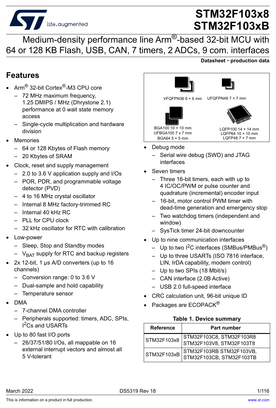
Specifications microcontroller
CoreARM Cortex-M3 CATALOG
Max frequency72 MHz CATALOG
Flash64 KB CATALOG
RAM20 KB CATALOG
GPIO37 CATALOG
Supply (min)2 V CATALOG
Supply (max)3.6 V CATALOG
Peripherals
TIM x4 (16-bit)ADC x2 (12-bit)USARTSPII2CCANUSB 2.0 FS
Provenance
Pin functions extracted by ds2sf from the ST datasheet (116 pages, sha256 0596dd57693c, source lcsc); Claude cites pages and refuses to fabricate, flagging muxed pins for review. CAD from KiCad official libraries (CC-BY-SA 4.0). Footprint pads carry KiCad
pinfunction/pintype. 3D board-context composed with cadquery (FR4 + copper pads + solder + pin 1) and rendered via step2glb. Datasheet: ST STM32F103x8/xB.